
$RYA (+1,56 %)
$UNH (-0,86 %)
$GM (-1,86 %)
$RTX (+1,67 %)
$UPS (+0,92 %)
$UNP (+1,7 %)
$NOC (-0,33 %)
$BA (+0,73 %)
$MC (-0,67 %)
$TXN (-0,14 %)
$STX (-10,53 %)
$SSAB A (+1,07 %)
$ASML (-0,53 %)
$GEV (+2,34 %)
$SBUX (-1,01 %)
$T (+5,29 %)
$GD (+0,86 %)
$MSCI (+1,18 %)
$META (-1,53 %)
$NOW (+1,19 %)
$IBM (+0,55 %)
$LRCX (-3,57 %)
$TSLA (+3,79 %)
$MSFT (-0,41 %)
$000660
$005930
$SAP (+0,64 %)
$ABBN (-0,33 %)
$DBK (+1,06 %)
$ROG (-0,99 %)
$DOW (+2,42 %)
$NDAQ (+0,03 %)
$LMT (+2,77 %)
$CAT (+0,09 %)
$TMO (-1,42 %)
$HON (+1,46 %)
$MA (+0,92 %)
$BX (+0,76 %)
$WM (+0,74 %)
$WDC (-11,03 %)
$SNDK
$V (+0,03 %)
$AAPL (+0,68 %)
$SOFI (-5,6 %)
$CL (+8,39 %)
$AXP (-0,37 %)
$XOM (+1,86 %)
$CVX (+4,28 %)
000
SK Hynix
Action
Action
ISIN: KR7000660001
Ticker: 000660
KR7000660001
000660
Price
Discussion sur 000660
Postes
96J·
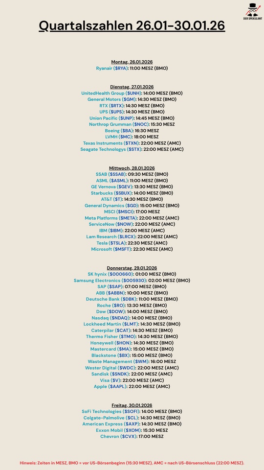
Quartalszahlen 26.01-30.01.2026
1414
7 Commentaires
der_Don@der_Don
6J
•
66
•Voir toutes les 3 autres réponses

3Sem.·
Strategy Update 2026
Hi folks,
I'm about to make a major strategic change to my portfolio this month. I have cracked the €120,000 mark 🎉 and have taken this as an opportunity to weatherproof my allocation for the coming years.
Here is my roadmap:
1. the tax "life hack": FIFO optimization 💡
I stop my previous core ETFs ($VHVG (+0,21 %) , $MEUD (-0,08 %) , $EXCH (-1,46 %) ) and leave them untouched. Why? In Germany, the FIFO principle (First-In-First-Out) applies. By saving new ISINs from now on (MSCI World ex-USA, NASDAQ 100 & MSCI EM), I "protect" my old shares with the high book profits. Later, I can sell the younger tranches first with less profit and massively defer the tax burden.
2nd core update: USA cap & EM limits 🌍
From now on, my core (approx. 74% of the portfolio) will be re-saved with €280 per month. I love US performance, but don't want any bulk risk:
USA cap: maximum 55% in the core.
Emerging markets: cap at 10%
3. satellite & venture: my high-conviction stocks
This area should make up 20% of my portfolio. Here I invest €400-600 per month in themes that I absolutely believe in. Currently in focus:
Cloudflare ($NET (-0,89 %) ): Infrastructure & cybersecurity are the basis of everything for me.
Siemens Energy ($ENR (-1,81 %) ): My play on the energy transition and grid expansion.
Hims & Hers ($HIMS) (-8,07 %)Exciting disruptor in the telehealth sector.
Tech from the Far East: With Xiaomi ($1810 (-1,86 %) ) and CATL ($3750 (+3,12 %) ) I cover important future markets.
Coinbase $COIN (-1,66 %) complements my direct Bitcoin holdings (target: 3.5% crypto share of the overall portfolio).
Other additional stocks are $NBIS (-9,18 %) , $000660 and $RKLB (-4,91 %)
4. the big goal: retirement in 2054 🏁 or perhaps even earlier
The math is done: I am aiming for a final capital of around € 780,000 by 2054. With a sustainable withdrawal rate of 4%, this will give me a monthly pension of around €2,600 without having to deplete the capital stock in the long term, thus closing my pension gap. It should be mentioned in the calculation that I calculate with a 5% return per year instead of the expected long-term return of 7-8% and therefore include a safety factor.
The whole thing is rounded off with a 3% share of gold (Euwax Gold II) and 17% bonds as a safety anchor.
What do you think of the FIFO tactic? Do you also use different ISINs for the same market in order to remain flexible in terms of tax, or is that too much "portfolio messing around" for you? 😉 And what do you think of my selection in the venture sector?
1515
6 Commentaires
I have also already consumed a lot of information on FiFo optimization. However, the usual recommendations for ETF switching there usually refer to the previous savings period, not to the capital paid in. Depending on the investment period, ISIN changes are common every 10 years. How long have you been saving in your existing core fund?
•
11
•
1Mo·
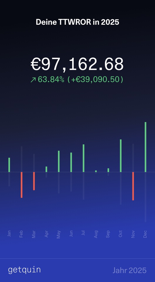
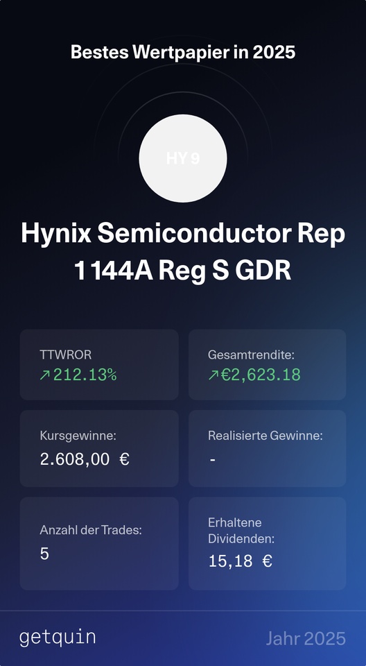
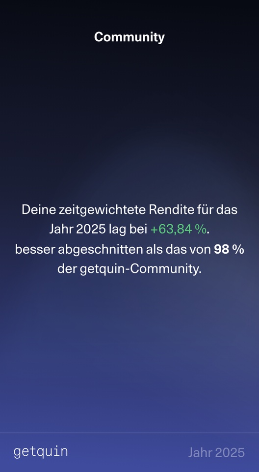
2025 Review: Goal achieved thanks to a strong core
I didn't have such high expectations this year, after last year went very well thanks to $RKLB (-4,91 %) went very well last year. Nevertheless, I was able to exceed my target of €80k and would like to thank above all $000660 (SK Hynix) and again to $RKLB (-4,91 %) for a great year-end rally.
I am still very convinced of SK Hynix and think it is undervalued, Rocket Lab has of course run very hot and will probably come down to earth again (as it did today).
Happy New Year to you all and good luck with your investments in 2026 🙏🏼
2323
3Mo·
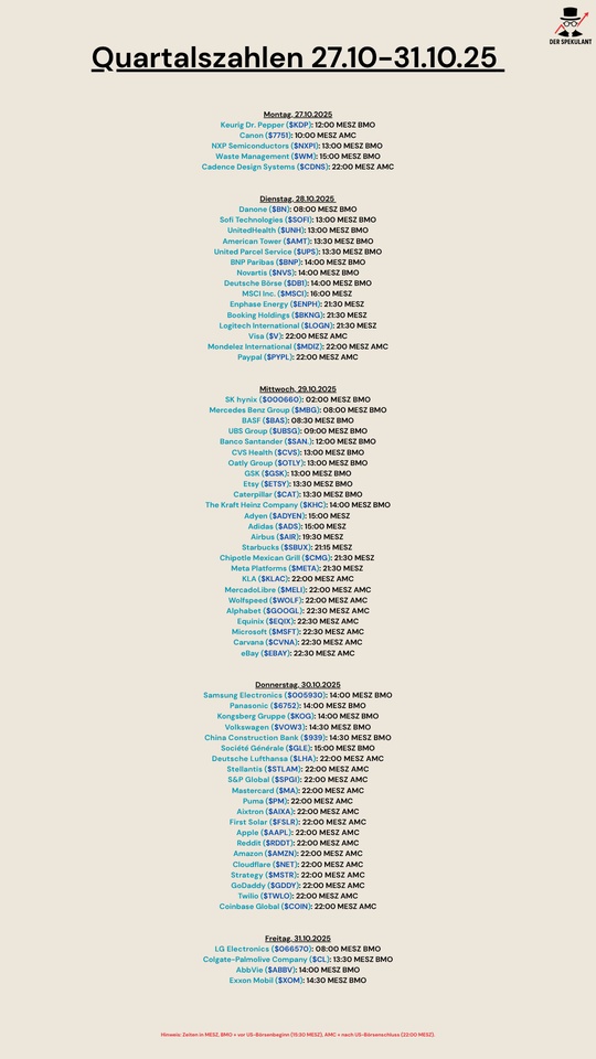
Quarterly figures 27.10-31.10.25
$KDP (+3,95 %)
$7751 (+1,39 %)
$NXPI (-2,55 %)
$WM (+0,74 %)
$CDNS (-1,07 %)
$BN (-2,55 %)
$SOFI (-5,6 %)
$UNH (-0,86 %)
$AMT (-0,12 %)
$UPS (+0,92 %)
$BNP (+0,25 %)
$NVS (+0,4 %)
$DB1 (+1,16 %)
$MSCI (+1,18 %)
$ENPH (-2,07 %)
$BKNG (-1,03 %)
$LOGN (-1,95 %)
$V (+0,03 %)
$MDLZ (+3,2 %)
$PYPL (+0,11 %)
$000660
$MBG (+0,41 %)
$BAS (-0,38 %)
$UBSG (-1,17 %)
$SAN (+0,85 %)
$CVS (+1,22 %)
$OTLY (+0,31 %)
$GSK (+2,39 %)
$ETSY (-2,57 %)
$CAT (+0,09 %)
$KHC (+3,9 %)
$ADYEN (-2,47 %)
$ADS (-2,03 %)
$AIR (-1,74 %)
$SBUX (-1,01 %)
$CMG (+0,12 %)
$META (-1,53 %)
$KLAC (-7,55 %)
$MELI (-2,07 %)
$WOLF (-8,3 %)
$GOOGL (+0,9 %)
$EQIX (+0,41 %)
$MSFT (-0,41 %)
$CVNA (-5,65 %)
$EBAY (-2,2 %)
$005930
$6752 (-0,26 %)
$KOG (+2,93 %)
$VOW3 (-0,75 %)
$GLE (+1,86 %)
$LHA (+0,1 %)
$STLAM (+1,05 %)
$SPGI (+0,78 %)
$MA (+0,92 %)
$PUM (-0,8 %)
$AIXA (-1,59 %)
$FSLR (+1,69 %)
$AAPL (+0,68 %)
$REDDIT (-0 %)
$AMZN (+0,15 %)
$NET (-0,89 %)
$MSTR (+5,33 %)
$GDDY (+2,42 %)
$TWLO (-1,79 %)
$COIN (-1,66 %)
$066570
$CL (+8,39 %)
$ABBV (+1,73 %)
$XOM (+1,86 %)


9Mo·
SK Hynix [ NVDA Supplier ] Q1'25 Earnings Highlights:
🔹 Revenue: ₩17.64T (Est. ₩17.2T) 🟢; UP +42% YoY
🔹 Operating Profit: ₩7.44T (Est. ₩6.62T) 🟢; UP +158% YoY
🔹 Net Income: ₩8.11T (Est. ₩5.04T) 🟢; UP +323% YoY
🔸 Overtook Samsung to become global No.1 in DRAM revenue and profitability in Q1
Segment & Operational Highlights:
🔹 DRAM Revenue Share: ~80%
🔹 DRAM Profitability Improved QoQ despite seasonal price weakness
🔹 NAND: Maintained profitability despite declining prices and volumes
🔹 Cash & Equivalents: ₩14.3T (UP ₩0.2T QoQ)
🔹 Debt Ratio: 29%, Net Debt Ratio: 11%
🔹 Operating Margin: 42% (vs. 23% YoY); UP +19pp YoY
🔹 Net Margin: 46%
Outlook & Guidance:
🔹 Q2 DRAM Sales: Expected to grow low-teens % QoQ
🔹 Q2 NAND Sales: Expected to grow over 20% QoQ
🔹 Maintains HBM demand projection: To double YoY in FY25
🔹 Capex: Slight increase YoY; remains disciplined and focused on ROI
🔹 eSSD Trend: Shift from 61TB to 122TB; developing 244TB QLC eSSD
🔹 AI-optimized eSSD demand (QLC/TLC) remains strong due to data center needs
Market Position:
🔹 Overtook Samsung to become global No.1 in DRAM revenue and profitability in Q1
🔹 HBM3E 12-layer chips to exceed 50% of HBM3E sales in Q2
🔹 Leading early mass production and customer qualifications for HBM4
🔹 DRAM mix shifting toward DDR5, 24Gb/32Gb chips
Strategic Developments:
🔸 Continued expansion of M15X fab to support AI memory scaling
🔸 AI-driven demand and DeepSeek models supporting long-term HBM growth
🔸 Entered LPCAMM2 production for AI PCs; SOCAMM2 for servers to follow
🔸 Strengthening supply chain collaboration amid global uncertainty
🔸 Proactive response to tariff-driven customer stockpiling; limited inventory concerns
Commentary:
🔸 CFO Kim Woo-hyun: “Tariffs and protectionist measures are making market forecasting increasingly difficult. We remain cautious yet flexible on Capex.”
🔸 “Despite macro volatility, HBM demand remains strong and predictable due to annual supply agreements.”
🔸 “Direct U.S. exports remain low; shipments for American clients are routed globally.”
Competitive Positioning:
🔸 “SK Hynix’s lead in AI memory and customized HBM solutions underpins our #1 position in DRAM.”
🔸 “We aim to maintain profit-led growth by focusing on high-margin, high-performance memory products.”
11
1Année·
SK Hynix Q4 '24 Earnings Highlights;
🔹 Operating Profit: ₩8.08T (Est. ₩8.03T) 🟢
🔹 Net Income: ₩8.00T (Est. ₩5.91T) 🟢
🔹 Revenue: ₩19.77T (Est. ₩19.77T) 🟡
Outlook:
🔹 1Q 2025 DRAM B/G: Low-teen% decrease QoQ
🔹 1Q 2025 NAND B/G: High-teen% decrease QoQ
🔹 2025 DRAM Market Outlook: Mid-to-high teen% growth
🔹 2025 NAND Market Outlook: Low-teen% growth
🔹 HBM Revenue: Expected to grow over 100% YoY in 2025
Q4 Segments:
🔹 HBM Revenue: Over 40% of total DRAM revenue in Q4, with HBM3E shipments beginning as planned.
🔹 DRAM ASP: Increased +10% QoQ due to a favorable product mix (HBM and DDR5).
🔹 NAND Revenue: Growth driven by enterprise SSD (eSSD) demand, though legacy products like DDR4 saw price declines.
Full-Year 2024 Financial Performance:
🔹 Operating Profit: ₩23.47T; UP +102% YoY
🔹 Revenue: ₩66.19T; UP +102% YoY
Capital Expenditures and Strategic Investments:
🔹 2025 Capex: Significant increase for new FAB infrastructure and HBM production.
🔹 Dividend Plan: Fixed annual dividend to increase by 25% during 2025-2027.
🔹 1Cnm Technology: Production ramp-up of DDR5 and HBM4 products to maintain competitive edge in high-performance DRAM.
Key Strategic Highlights:
🔸 AI-Driven Growth: Strong demand for HBM products driven by AI servers and GPUs like NVIDIA’s Blackwell expected in 2025-2026.
🔸 General DRAM Shift: Reduced DDR4/LPDDR4 production to single-digit revenue share in 2025, focusing on DDR5 and HBM profitability.
🔸 Customer Alignment: Securing long-term agreements for HBM supply and aligning investments with hyperscale customers’ AI priorities.
🔸 China Concerns: Continued market dominance in advanced DRAM and HBM as Chinese manufacturers face challenges in producing high-performance memory products.
44

1Année·
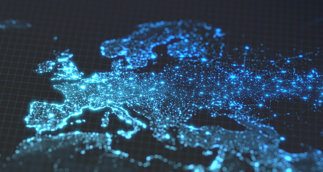
Europe hopelessly left behind? 🇪🇺📉
I would like to initiate a discussion on the occasion of the recently announced 500 billion dollar Stargate project in the USA.
Do you think it is possible for Europe to catch up with the existing technological backlog? Or is "Stargate" the final nail in the coffin? And which countries do you see at the forefront of the AI age in the future?
For me, these countries are on the winning side:
USA 🇺🇸 - The USA has been at the forefront of technology right from the start. OpenAI (ChatGPT), Alphabet $GOOGL (+0,9 %) (Gemini), Meta $META (-1,53 %) Microsoft $MSFT (-0,41 %) .... The list of companies relevant to the industry is long. Nowhere else in the world is more invested in AI. "Stargate" will now increase this imbalance many times over
China 🇨🇳 - China acts independently of the West and yet is still a major player with companies such as Tencent $TCEHY (-3,02 %) , Alibaba $BABA (-1,51 %) , Huawei, Xiaomi $1810 (-1,86 %) and Baidu $9888 (-1,82 %) are ideally positioned. Chinese companies are fast and innovative. The gigantic subsidies from the Chinese government also play a decisive role in this context. Another advantage is that the Chinese are currently receiving energy from Russia virtually as a gift.
Japan 🇯🇵 - With SoftBank, Japan has $9984 (-1,72 %) a real AI champion in its country. In Japan, NVIDIA and SoftBank $NVDA (+0,21 %) and SoftBank are building a joint innovative AI infrastructure. The fact that SoftBank and OpenAI are to be the lead partners in the Stargate project and that Masayoshi Son (CEO of SoftBank) will chair the new company will benefit Japan. The huge assets that are being built up there will flow back into the home country in one way or another. The close cooperation with the government (+high subsidies), the leading position in robotics and the recent developments in the semiconductor industry should also be noted.
Singapore 🇸🇬 - Very small country, lots of money, very good government, very well-educated population, lots of expats, lots of foreign investment, very few logistical challenges as a city state...... So things are looking VERY good for Singapore.
UAE 🇦🇪 /Saudi Arabia 🇸🇦/Qatar 🇶🇦 - Rich Gulf states that will invest billions in AI projects abroad (e.g. UAE participation in "Stargate"). They will generate large returns on these investments, while at the same time investing in the digitalization of their own country, thereby bringing great prosperity to their relatively small populations. Although there is also a large expat community in the UAE, including in the field of AI, I think that the Gulf states will mainly benefit from their investment funds.
I am unsure about these countries unsure:
Canada 🇨🇦 - Canada is innovative and wealthy, but there are not really any relevant companies in the AI sector. In addition, the universities are middle class and they lose a lot of talent to their neighbor, the USA. However, the country has potential, also because it is very attractive for foreign specialists.
Taiwan 🇹🇼 - TSMC $2330 from Taiwan supplies the world with chips, including those urgently needed for AI, but the country's heavy dependence on a single company, which has recently been expanding abroad (especially Japan and the USA), poses a risk. The development of the conflict with China and the possible success of Rapidus from Japan and Samsung in the field of 2nm chips will also be decisive for Taiwan's future in the field of AI.
South Korea 🇰🇷 - Technological leader, politically unstable. Companies like Samsung $005930 and SK Hynix $000660 from South Korea are leaders in the field of AI. There is a great deal of expertise in the country and the government is also supporting the transformation. However, I am unsure about the excessive dependence on the chaebols (e.g. Samsung), which account for an unhealthily large proportion of economic output. The dysfunctionality of the rule of law due to corrupt politicians and courts, the recent very tense domestic political situation and the constant threat from neighboring North Korea should also be viewed critically.
India 🇮🇳 - The next few years will show whether India can become the new China. India is growing dynamically and, with its 1.4 billion inhabitants, has a huge potential workforce, but it is still heavily dependent on foreign know-how. India is not as innovative as developed countries and has to deal with domestic challenges such as hunger, which could make investment in AI more difficult. Indian companies are very open to AI and are trying to adapt it quickly, but developing it is another matter.
The Netherlands 🇳🇱 - With ASML $ASML (-0,53 %) the Netherlands is home to one of the most important companies when it comes to AI. Without ASML's machines, the particularly advanced chips required for AI could not be produced. This puts the Netherlands, with its small population, in a rather comfortable position. However, it is also heavily dependent on a single company, which is also increasingly being targeted by geopolitics, with the result that the USA regularly blackmails the Netherlands to dictate where it has to deliver these machines. Recently, there have also been developments that threaten ASML's monopoly.
Germany 🇩🇪 - Germany is good at AI research, but there is a lack of AI champions. Companies such as Siemens $SIE (-0,9 %) are doing well in terms of industrial AI and SAP is also $SAP (+0,64 %) is investing heavily in its own AI, but there is still no sign of a German export hit in the field of AI. There is also a massive lack of investment in AI infrastructure and politicians are blocking rather than promoting. There is a general lack of a national vision, a combination of strategic policy and large-scale private investment, as is the case in other countries. The EU is also more of an obstacle to new investments. The concept of joint ventures is also used less in this country, although this could help to pool knowledge and resources in order to make a difference for one's own country. So all is not lost, but a political reorientation and new entrepreneurial courage are needed to catch up, which is getting bigger every day.
France 🇫🇷 - The French are also innovative and have an AI star in their country with Mistral AI, but they have similar problems to the Germans. Politics at national and EU level and the lack of major investments and new infrastructure are paralyzing the country.
UK 🇬🇧 - With universities such as Oxford and Cambridge, the UK has been conducting top-level research for a long time, including in the field of AI. They are innovative with many expats from abroad, although recently less from continental Europe. Unfortunately, however, they do not have any notable tech companies to call their own. Two of the most innovative tech companies and British hopefuls, ARM $ARM (-1,93 %)
and Graphcore, are now both owned by the aforementioned Japanese SoftBank Group, but this does not mean that the UK can no longer benefit from the positive development of these companies. Nevertheless, they are no longer British.
ConclusionIt will not be easy for Europe to catch up. The competitors are mostly fast, very financially strong, innovative and led by visionaries. We cannot compete with a fragmented capital market, slow decision-making processes and bureaucrats from Brussels. However, it is also clear that the potential is there. We (still) have many bright minds here, but without a fundamental change in policy, decisive reforms and some pioneering spirit, I believe it will be impossible to catch up. The window of opportunity is getting smaller.
How do you see it all? Do you disagree somewhere or are you missing an important country?

1616
11 CommentairesEurope is dead.
We are transferring our entire wealth to the Americans.
People invest billions of their hours (free time) to watch free advertising on instagram, YouTube and co. And they are still training their ML models.
We can no longer catch up :)
We are transferring our entire wealth to the Americans.
People invest billions of their hours (free time) to watch free advertising on instagram, YouTube and co. And they are still training their ML models.
We can no longer catch up :)
•
99
•
1Année·
From sand to chip: how is a modern semiconductor made?
Reading time: approx. 10min
1) INTRODUCTION
Since 2023 at the latest and the rapid rise of Nvidia $NVDA (+0,21 %) semiconductors and "AI chips" in particular have been the talk of the town. Since then, investors have been chasing after almost every company that has something to do with the manufacture of chips, driving share prices to unimagined heights. However, hardly any investors really know how complex the value chain is within the production of modern chips.
In this article, I will give you an overview of the entire manufacturing process and the companies involved. Even if many of you have a vague idea that the production of modern chips is complex, you will certainly be surprised by how complex it really is in reality.
2) BASIC
The starting point for every chip are so-called wafers [1] - i.e. thin wafers, which usually consist of so-called high-purity monocrystalline silicon. In the field of power semiconductors, which primarily comprises chips for applications with higher currents and voltages, silicon carbide (SiC) or galium nitride (GaN) has recently also been used as the base material for the wafers.
In the so-called front end the actual core components of the chips - the so-called dies - are created and applied to the wafers. The dies are rectangular structures that contain the actual functionality of the later chip. The finished dies are then tested for their functionality and electrical properties. Each die that is found to be good is then integrated into the so-called backend where the individual dies are separated on the wafer. This is followed by the so-called packaging. The individual dies from the front end are then electrically contacted and integrated into a protective housing. In the end, this housing with the contacted die is what is usually called a chip chip.
Now that we have a rough overview of the overall process, let's take a closer look at the individual processes involved in producing the dies on the wafer. This is the area in which most highly complex machines are used and which is usually the most sensitive.
3) FROM SAND TO WAFER
Before wafers made of high-purity silicon can even be produced and the actual process for manufacturing dies can begin, the actual wafer must first be manufactured in almost perfect quality. To do this, quartz sand, which consists largely of silicon dioxide, is reduced with carbon at high temperatures. This produces so-called raw siliconwhich, with a purity of around 96%, is not yet anywhere near the quality required for the production of wafers.
In several chemical processes, which are carried out by Wacker Chemie
$WCH (-0,26 %) or Siltronic
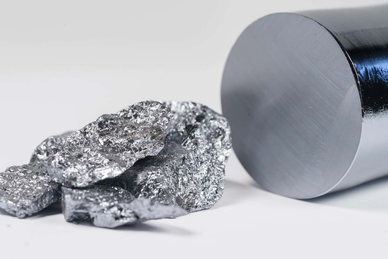
$WAF (+0,24 %) are used to turn the "impure" silicon into so-called polycrystalline silicon with a purity of 99.9999999%. For every billion silicon atoms, there is then only one foreign atom in the silicon. However, this pure polycrystalline silicon is still not suitable for the production of wafers, as the crystal structure in the silicon is not uniform enough. In order to create the right crystal structure, the polycrystalline silicon is then melted again and a so-called ingotwhich is made from monocrystalline silicon is produced. A comparison between raw silicon and the ingot can be found in the following image [3]:
This ingot is then sawn into thin slices, which are then the final wafers for semiconductor production. The best-known wafer producers are Shin Etsu
$4063, (+3,12 %)
Siltronic or GlobalWafers
$6488.
4) FROM THE WAFER TO THE DIE
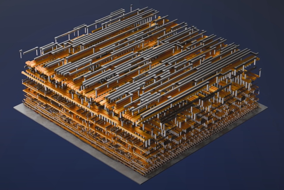
The wafers described in the previous section can now be used to produce dies. The overall process for producing dies basically consists of applying a large number of layers using various chemical, mechanical and physical processes. The overall process (depending on the product) takes approx. 80 different layers on the wafer, requiring almost 1000 different process steps and 3 months
non-stop production are required [4].
A macroscopic analogy is useful here, which I have also taken from [4]. You can compare the overall process for producing dies with baking a large multi-layer cake. This cake has 80 layers and the recipe for baking consists of 1000 steps. It takes 3 months to make the cake and if even one layer of the cake deviates from the recipe by more than 1%, the whole cake collapses and has to be thrown away.
In the first process steps, the wafer is covered with billions tiny little transistors are created on the wafer, which are then all individually electrically contacted in the following steps. The final steps consist of electrically connecting the transistors to each other, resulting in a complete electrical circuit [4]:
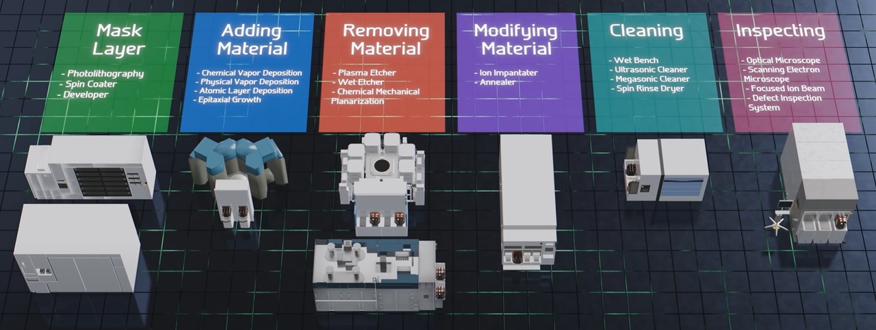
Each individual layer of the approximately 80 layers in the die requires highly specialized processes, which can be roughly summarized as:
- Applying masks: Photolithography, photoresist coating (applying photoresist)
- Apply material: Chemical Vapor Deposition (CVD), Physical Vapor Deposition (PVD), Atomic Layer Deposition
- Remove material: Plasma annealing, Wet annealing, Chemical Mechanical Planarization (CMP)
- Modify material: Ion Implanting, Annealing
- Material cleaning
- Inspecting the layers: Optical, Microscopical, Focused Ion Beam, Defect Inspection
Apply masks
Ultimately, a mask can be thought of as an enlarged copy of the structure of a special layer in the die. These so-called photomasks are then scanned using so-called scanners or steppers "copied" in reduced size onto the wafer. The best-known manufacturer of such lithography systems is ASML
$ASML (-0,53 %). It is currently the only producer of lithography systems that make it possible to produce structures smaller than 10 nanometers on the wafer. In today's powerful and modern chips, such as those found in smartphones, AI chips and processors, the smallest structures are around 3 nanometers in size. Other manufacturers of lithography systems for larger structures (10nm and larger) are Canon Electronics
$7739 or Nikon $7731 (+1,08 %) .
The photomasks - i.e. the enlarged "copies" of the structures - are produced by companies such as Toppan $7911 (+0 %) , Dai Nippon Printing
$7912 (+1 %) or Hoya $7741 (+3,59 %) manufactured. Systems for cleaning the photomasks or for applying the photoresist are produced, for example, by Suss Microtec
$SMHN (+4,39 %) for example.
Apply/remove/modify/clean material
As can be seen in the overview above, there are a variety of methods and processes for modifying the material of a particular layer. As a result, there is a lot of different equipment that can handle a process very well with incredible specialization. The best-known and most successful equipment manufacturers include Applied Materials $AMAT (-2,73 %), LAM Research
$LRCX (-3,57 %), Tokyo Electron (TEL)
$8035, (-1,1 %)
Suss Mictrotec, Entegris
$ENTG (-2,82 %) and Axcelis $ACLS (-3,61 %).
The material - for example, highly specialized chemicals - is of course also required for production. Companies such as Linde
$LIN (+2,12 %), Air Liquide
$AI (-0,85 %), Air Products
$APD (+6,8 %) and Nippon Sanso
$4091 (+1,72 %) are major manufacturers of process gases such as nitrogen, hydrogen and argon.
Inspect
As mentioned, every single layer in the manufacturing process of a die must be perfect in order to obtain a functional die at the end. Any small deviation or foreign particles can impair the functionality of the die. As the function of the die can only be checked precisely on the finished die, it is advantageous to inspect the individual layers for defects and deviations during production. Special machines are required for this, which must be able to do different things depending on the layer. Manufacturers of such machines include KLA
$KLAC (-7,55 %) or Onto Innovation
$ONTO (-2,82 %).
The following applies to almost all of the companies mentioned in this section: the companies are highly specialized and have quasi-monopolies on the machines for certain process steps. quasi-monopolies. Suitable equipment therefore usually costs several million dollars. In addition, some of the systems are so complex that they can only be serviced by the manufacturer's own service staff, which results in recurring service revenues for every machine sold. As a rule, each machine requires several highly specialized engineers to ensure long-term stable operation.
5) FROM THE DIE TO THE FINISHED CHIP
Once the wafer has been processed, the dies on the wafer are checked for functionality. There is highly specialized equipment for this, so-called probers. These probers test each individual chip several times, if necessary, to check the functionality implemented in the design. Manufacturers of such probers include Teradyne $TER (-3,18 %), Keysight Technologies
$KEYS (-1,17 %), Onto Innovation or Tokyo Electron. These probers have to control each individual die, some of which are only a few square millimetres in size, and contact the corresponding much smaller test structures with tiny needles. The testing process is sometimes outsourced to entire companies that offer die testing as a complete package. One example of such providers is Amkor Technology
$AMKR (-2,51 %).
The processed and tested wafer is now sawn to obtain individual dies. The dies that are found to be good are then integrated into a protective housing in the backend. The dies that have not passed the functionality test are either sorted out or (depending on the error pattern) processed as a variant with reduced functionality similar to those with full functionality. After a final functional test in the package, the chip is ready for use.
6) FOUNDRIES, FABLESS & SOFTWARE
Now that we have an overview of the complex process of manufacturing a chip, let's zoom out a little further to understand which companies perform which tasks in the semiconductor industry.
It's funny that not once in the manufacturing process has the name Nvidia $NVDA (+0,21 %) or Apple $AAPL (+0,68 %) has been mentioned? Yet they have the most advanced chips, don't they?
The pure production of the chips is done by other companies - so-called foundries. Companies like Nvidia and even AMD $AMD (-4,77 %) are in fact fablessThis means that they do not have their own production facilities but only supply the chip design and let the foundries manufacture the actual chip according to their design.
The design of a chip is like the blueprint for production - the foundries then take over the recipe creation and the actual production. There is special software for designing chips. Companies known for this software include Cadance Design
$CDNS (-1,07 %) and Synopsys $SNPS (-2,52 %). But also the industrial giant Siemens
$SIE (-0,9 %) now also supplies software for designing integrated circuits. Synopsys also offers other software for data analysis within foundry production.
Speaking of foundries; the best known foundry is probably TSMC
$TSM, (-1,59 %) which is the global market leader in foundries. TSMC designs itself no chips itself and specializes exclusively in the production of the most advanced generations of chips. Another major player that also masters the most advanced structure sizes is Samsung $005930. In contrast to TSMC manufactures Samsung also produces its own designs. Other large foundries are Global Foundries
$GFS, (-4,15 %) which was originally a spin-off from AMD and the Taiwanese company United Micro Electronics
$UMC. (-3,12 %)
The best-known fabless companies - i.e. companies without their own chip production - are Nvidia, Apple, AMD, ARM Holdings
$ARM, (-1,93 %)
Broadcom $AVGO (+1,35 %), MediaTek $2454 and Qualcomm $QCOM. (+0,96 %) In the meantime Alphabet $GOOGL, (+0,9 %)
Microsoft $MSFT, (-0,41 %)
Amazon $AMZN (+0,15 %) and Meta $META (-1,53 %) have designed their own chips for certain functionalities and then have them manufactured in foundries.
In addition to foundries and fabless companies, there are of course also hybrid models, i.e. companies that take on both production and design. The best-known examples of this are, of course, companies such as Intel
$INTC (-3,29 %) and Samsung. There is also a whole range of so-called Integrated Device Manufacturer (IDM)which for the most part only manufacture their own designed chips and do not accept customer orders for production. Well-known companies such as Texas Instruments
$TXN, (-0,14 %)
SK Hynix
$000660,
STMicroelectronics
$STMPA, (-0,77 %)
NXP Semiconductors
$NXPI, (-2,55 %)
Infineon $IFX (-2,55 %) and Renesas $6723 (-1,93 %) are among the IDMs.
FINAL WORD
The aim of this article was to provide an overview of the complexity of the semiconductor industry. I do not, of course no claim to be complete, as there are of course many other companies that are part of this value chain. As Getquin thrives on active exchange, I'll give you some food for thought to discuss in the comments below the article:
- feel free to link any other companies in the comments if you think I've forgotten any relevant ones
- what was the most surprising new information for you from the article?
- which companies from the article have you never heard of?
- before reading the article, did you know approximately how a modern chip is produced and what steps are necessary for this?
In general, I can recommend the 20-minute YouTube video at [4] to any interested reader. It provides an excellent animated overview of the manufacturing process of modern chips.
Stay tuned,
Yours Nico Uhlig (aka RealMichaelScott)
SOURCES:
[1] Wikipedia: https://de.wikipedia.org/wiki/Wafer
[2] https://www.halbleiter.org/waferherstellung/einkristall/
[3] https://solarmuseum.org/wp-content/uploads/2019/05/solarmuseum_org-07917.jpg
[4] Branch Education on YouTube: "How are Microchips Made?" https://youtu.be/dX9CGRZwD-w?si=xeV0TYgJ2iwNOKyO


Titres populaires
Meilleurs créateurs cette semaine
Données en temps réel par LSX · Données financières de FactSet