After my first post on humanoid robots received a lot of positive feedback, I went into more detail. I have subsequently added my favorites in each sector.
Extended analysis of the value chain including shovel manufacturers and potential hidden champions
New categorySecondary key sectors (sales, marketing, financing)
In additionTop 25 companies worldwide, as well as Top 10 Europe and Top 10 Asia
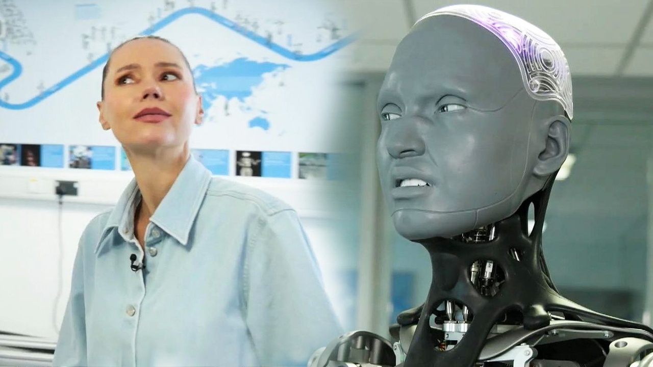
I have also added a video link for beginners. This will give you an idea of how far the development of humanoid robotics has already progressed.
https://www.stern.de/panorama/wissen/humanoider-roboter---wie-reagiert-er-auf-beleidigungen--35996156.html
Thank you for your attention and your support 🙏
🌐 1. value chain of humanoid robots (with hidden champions)
1. research & chip design
$ARM (+9.34%) ARM (UK) - CPU-IP, energy-efficient processors
$SNPS (+8.51%) Synopsys (US) - EDA software, chip design
$CDNS (+4.98%) Cadence (US) - EDA & Simulation
$PTC PTC (US) - Engineering Software, CAD/PLM
$DSY (+1.11%) Dassault Systèmes (FR) - 3D Design & Digital Twin
$SIE (+0.85%) Siemens (DE) - Industrial Software & Lifecycle Mgmt
$ADBE (+1.89%) Adobe (US) - Design, AR/UX
ANSYS (US) - multiphysical simulation - acquisition by Synopsis
Altair (US) - CAE, simulation, digital twin - acquisition by Siemens
$HXGBY (-1.05%)
Hexagon (SE) - Metrology & Simulation
$AWE Alphawave IP Group (UK) - High-speed chip IP for AI/robotics
1.Synopsis, 2.Siemens and 3.Adobe are my top 3 in this sector
2. manufacturing technology & equipment
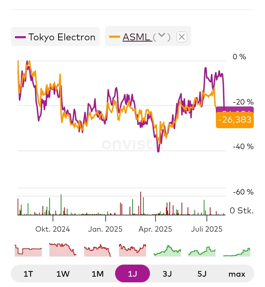
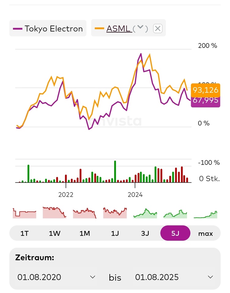
$ASML (+2.14%) ASML (NL) - Lithography (EUV)
$AMAT (+2.71%) Applied Materials (US) - Semiconductor equipment
$8035 (+2.15%) Tokyo Electron (JP) - wafer fabrication
$KEYS (-0.2%) Keysight Technologies (US) - Metrology
$6857 (+7.32%) Advantest (JP) - Chip test systems
$TER (+4.36%) Teradyne (US) - test systems + cobots
$6954 (+4.76%) Fanuc (JP) - Industrial robots, CNC
$CAT (-0.98%) Caterpillar (US) - autonomous machines
$KU2G KUKA (DE) - industrial robots
Comau (IT) - automation - not listed on the stock exchange
$ROK Rockwell Automation (US) - industrial automation
$JBL (+0.59%) Jabil (US) - contract manufacturing (EMS/ODM)
$KIT (+12.62%) Kitron (NO) - European EMS/ODM manufacturer
$AIXA (+2.78%) Aixtron (DE) - deposition equipment for compound semiconductors
$LRCX (+3.58%)
Lam Research (US) - Etch/deposition systems
$MKSI (-0.17%)
MKS Instruments (US) - Plasma/vacuum technology
$ASM (+2.02%)
ASM International (NL) - Deposition systems
1.ASML, 2.Keysight Technologies, 3.Fanuc are my top 3 in this sector
3. chip manufacturing (foundries)
$TSM (+4.89%) TSMC (TW) - leading foundry
$SMSN Samsung Electronics (KR) - foundry + memory
$GFS (-3.14%) GlobalFoundries (US) - specialty chips
$INTC (+7.11%)
Intel Foundry Services (US) - new western foundry player
$981
SMIC (CN) - largest Chinese foundry
$UMC
UMC (TW) - Power/RF/Embedded chips
1.TSMC, 2.Intel, 3.Samsung Electronics are my top 3 in this sector
4. computing & control unit ("brain")
$NVDA (+4.29%) Nvidia (US) - GPUs, AI chips
$INTC (+7.11%) Intel (US) - CPUs, FPGAs
$AMD (+9.4%) AMD (US) - CPUs, GPUs
$MRVL (-1.65%) Marvell (US) - Network Chips
$MU (+2.38%) Micron (US) - Memory
$DELL (+1.06%) Dell Technologies (US) - Edge & Infrastructure
Graphcore (UK) - AI chips (IPU) - not a listed company
Cerebras (US) - Wafer-scale engine - not a listed company
SiPearl (FR) - European HPC chip - not a listed company
1.Nvidia, 2.Marvell, 3.Micron are my top 3 in this sector
5. sensors ("senses")
$6758 (-1.15%) Sony (JP) - image sensors
$6861 (+3.6%) Keyence (JP) - Industrial sensors
$STM (+0.7%) STMicroelectronics (FR/IT) - Sensors, MCUs
$TDY Teledyne (US) - optical/infrared sensors
$CGNX (-0.02%) Cognex (US) - Machine Vision
$HON (-0.65%) Honeywell (US) - sensor technology, security
ANYbotics (CH) - autonomous sensor fusion - not a listed company
$AMBA (+8.59%) Ambarella (US) - video & computer vision SoCs for real-time image recognition
$OUST
Velodyne Lidar (US) - Lidar sensors - acquisition by Ouster
$AMS (-7.48%)
OSRAM (AT/DE) - optical sensors
1.Teledyne, 2.Keyence, 3.Ouster are my top 3 in this sector
6. actuators & power electronics ("muscles")
$IFX (+2.45%) Infineon (DE) - Power Electronics
$ON (+0.44%) onsemi (US) - Power & Sensors
$TXN (-1.66%) Texas Instruments (US) - Mixed-Signal Chips
$ADI (-0.12%) Analog Devices (US) - Signal Processing
$PH Parker-Hannifin (US) - Hydraulics/Pneumatics
$MP (-4.4%) MP Materials (US) - Magnets
$APH (-0.47%) Amphenol (US) - Connectors
$6481 (+0%) THK (JP) - Linear guides & actuators
$6324 (+5.98%)
Harmonic Drive (JP) - Precision gears & servo drives for robotics
$6594 (+2.49%)
Nidec (JP) - Electric motors
$6506 (+0.91%)
Yaskawa (JP) - Drives & Robotics
$SU (+2.59%)
Schneider Electric (FR) - Energy & control solutions
$ZIL2 (-0.36%)
ElringKlinger (DE) - Battery & fuel cell technology, lightweight construction
1.Parker-Hannifin, 2.MP Materials, 3.Infinion are my top 3 in this sector
7. communication & networking ("nerves")
$QCOM (+11.02%) Qualcomm (US) - mobile communications, edge AI
$ANET (+2.13%) Arista Networks (US) - Networks
$CSCO (+0.44%) Cisco (US) - Networks, Security
$EQIX (-0.5%) Equinix (US) - Data centers
NTT Docomo (JP) - 5G/6G carrier - not a listed company
$VZ Verizon (US) - Telecommunications
$SFTBY SoftBank (JP) - Carrier + Robotics
$ERIC B (-0.12%)
Ericsson (SE) - 5G/IoT infrastructure
$NOKIA (+1.16%)
Nokia (FI) - 5G/6G for industry
$HPE (+0.29%)
Juniper Networks (US) - Network technology - acquisition by HP
1.Arista Networks, 2.SoftBank, 3.Cisco are my top 3 in this sector
8. energy supply
$3750 (-1.23%) CATL (CN) - Batteries
$6752 (-1.17%) Panasonic (JP) - Batteries
$373220 LG Energy (KR) - Batteries
$ALB (-1.74%) Albemarle (US) - Lithium
$LYC (-1.6%) Lynas (AU) - Rare earths
$UMICY (+1.43%) Umicore (BE) - recycling
WiTricity (US) - inductive charging - not a listed company
$ABBN (+0.58%) Charging (CH) - charging infrastructure
$SLDP
Solid Power (US) - Solid state batteries
Northvolt (SE) - European batteries - not a listed company
$PLUG
Plug Power (US) - fuel cells
$KULR (-0.95%)
KULR Technology (US) - Thermal management & battery safety for mobile systems
1.Albemarle, 2.CATL, 3.Panasonic are my top 3 in this sector
9. cloud & infrastructure
$AMZN (+3.03%) Amazon AWS (US) - Cloud, AI
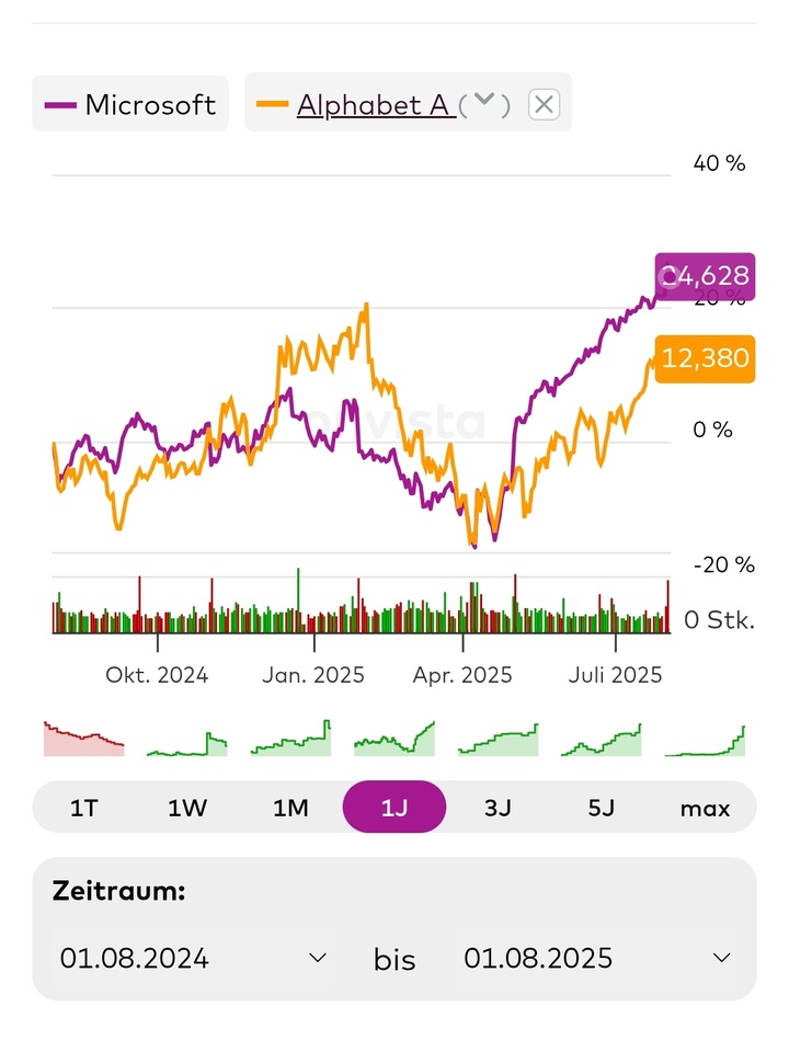
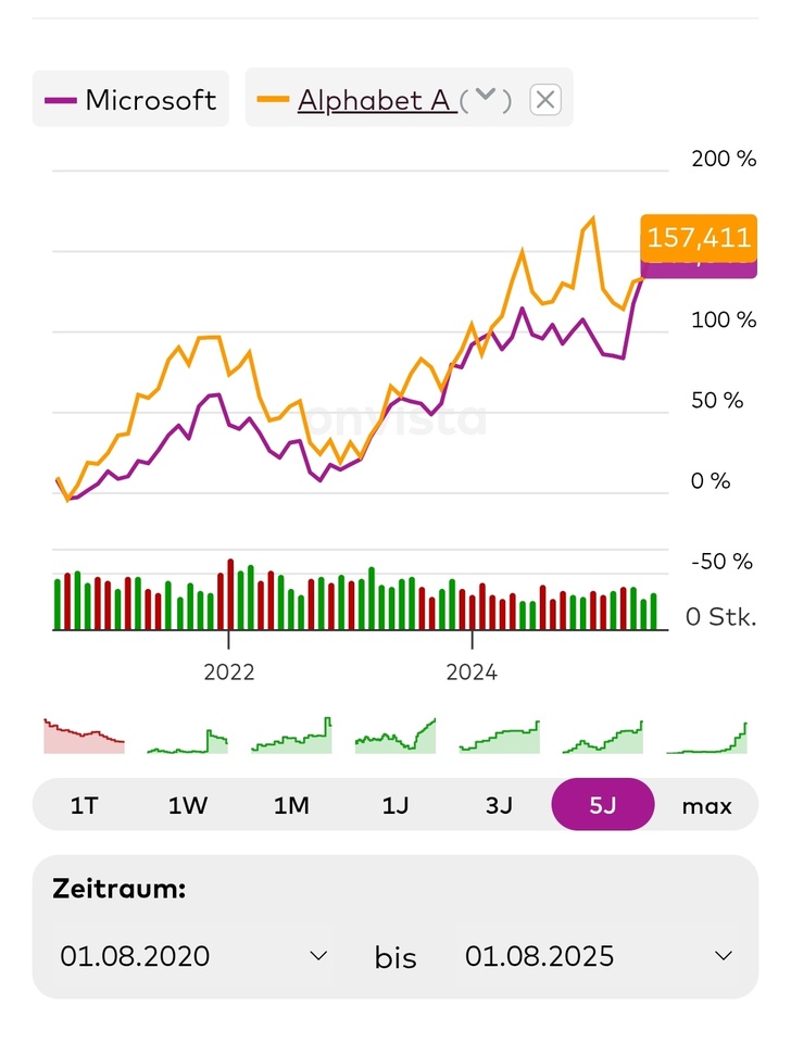
$MSFT (+1.38%) Microsoft Azure (US) - Cloud, AI
$GOOG (+1.06%) Alphabet Google Cloud (US) - Cloud, ML
$VRT (+0.73%)
Vertiv Holdings (US) - Data center infrastructure (UPS, cooling, edge)
$ORCL (-3.27%)
Oracle Cloud (US) - ERP + Cloud
$IBM (-0.2%)
IBM Cloud (US) - Hybrid cloud + AI
$OVH (+0.42%)
OVHcloud (FR) - European cloud
1.Alphabet, 2.Microsoft, 3.Oracle are my top 3 in this sector
10. software & data platforms
$PLTR (+0.13%) Palantir (US) - Data integration
$DDOG (+0.45%) Datadog (US) - Monitoring
$SNOW (-5.76%) Snowflake (US) - Data Cloud
$ORCL (-3.27%) Oracle (US) - Databases, ERP
$SAP (+1.3%) SAP (DE) - ERP systems
$SPGI S&P Global (US) - financial/market data
ROS2 Foundation - robotics middleware - not listed on the stock exchange
$NVDA (+4.29%) NVIDIA Isaac (US) - robotics development - part of Nvidia
$INOD (-3.14%) Innodata (US) - data annotation & AI training data
$PATH (+1.74%)
UiPath (RO/US) - Robotic process automation
$AI (+0.27%)
C3.ai (US) - AI platform
$ESTC (+0.13%)
(NL/US) - Search & data analysis
1.S&P Global, 2.Palantir, 3.Datadog are my top 3 in this sector
11. end applications / robots
$ABBN (+0.58%) ABB (CH/SE) - Industrial Robots
$6954 (+4.76%) Fanuc (JP) - Industrial robots
$TSLA (+0.55%) Tesla Optimus (US) - humanoid robot
$9618 (+0.73%) JD.com (CN) - logistics robot
$AAPL (-0.73%) Apple (US) - Platform & UX
$700 (-0.13%) Tencent (CN) - Platform & AI
$9988 (+3.39%) Alibaba (CN) - logistics & platform
PAL Robotics (ES) - humanoid robots - not a listed company
Neura Robotics (DE) - cognitive humanoid robots - not a listed company
$TER (+4.36%) Universal Robots (DK) - cobots - belongs to the Teradyne Corporation
Engineered Arts (UK) - humanoid robots - not a listed company
$ISRG (+0.63%) Intuitive Surgical (US) - surgical robotics
$GMED (+0.21%)
Globus Medical (US) - surgical robotics (ExcelsiusGPS platform)
$7012 (-1.31%) Kawasaki Heavy Industries (JP) - industrial robots, automation
$CPNG (-0.81%) Coupang (KR) - Logistics end user
$IRBT
iRobot (US) - consumer robotics (e.g. Roomba), non-humanoid, but navigation/sensor fusion
Boston Dynamics (US) - humanoid & mobile robots-no listed company
Hanson Robotics (HK) - humanoid robots (Sophia) - not a listed company
Agility Robotics (US) - humanoid robot "Digit" - not a listed company
1.Apple, 2.Tencent, 3.Alibaba are my top 3 in this sector
🛠 2. cross enablers (shovel manufacturers) - with hidden champions
Raw materials & battery materials
Albemarle - Lynas - Umicore
$SQM
SQM (CL) - Lithium
$ILU (-0.84%)
Iluka Resources (AU) - Rare earths
$ARR (+2.04%)
American Rare Earths (US/AU) - New supply chains
my number 1 in the sector is Albemarle
manufacturing technology
ASML - Applied Materials - Tokyo Electron
$LRCX (+3.58%)
Lam Research (US) - Plasma/etching processes
$ASM (+2.02%)
ASM International (NL) - ALD equipment
$MKSI (-0.17%)
MKS Instruments (US) - Plasma/vacuum technology
my number 1 in the sector is ASML
Quality assurance
Keysight - Advantest - Teradyne
$EMR (-1.36%)
National Instruments (US) - Measurement technology - from Emerson Electric adopted
$300567
ATE Test Systems (CN) - test systems
$FORM (+3.06%)
FormFactor (US) - Wafer probing
my number 1 in the sector is Keysight
Motion & Drive
Parker-Hannifin
Festo (DE) - Pneumatics, Soft Robotics - not a listed company
Bosch Rexroth (DE) - Drives, Controls - not a listed company
$6481 (+0%)
THK (JP) - Linear guides
my number 1 in the sector is Parker-Hannifin
Sensors/Imaging
$TDY Teledyne
$BSL (-0.34%) Basler (DE) - Industrial cameras
FLIR (US) - Thermal imaging sensors - acquisition by Teledyne
ISRA Vision (DE) - Machine Vision - not a listed company
my number 1 in the sector is Teledyne
Magnets & Materials
MP Materials
$6501 (+0.27%)
Hitachi Metals (JP) - Magnetic materials
VacuumSchmelze (DE) - Magnetic materials - not a listed company
$4063 (+2.39%)
Shin-Etsu Chemical (JP) - Specialty materials
my number 1 in the sector is MP Materials
Chip Design & Simulation
Synopsys - Cadence - ARM
$SIE (+0.85%)
Siemens EDA (DE/US)-Mentor Graphics-strategic business unit of Siemens AG
Imagination Tech (UK) - GPU-IP - not a listed company
$CEVA (+17.06%)
CEVA (IL) - Signal Processor IP
my number 1 in the sector is Synopsys
Engineering & Lifecycle
PTC - Dassault - Siemens
Altair (US) - Simulation - no longer a listed company
$HXGBY (-1.05%)
Hexagon (SE) - Metrology
$SNPS (+8.51%)
ANSYS (US) - Simulation - takeover by Synopsys
my number 1 in the sector is Siemens
Networks & Data Centers
Arista - Cisco - Equinix
$HPE (+0.29%)
Juniper (US) - Networks - Acquisition of HPE
$DTE (+0.51%)
T-Systems (DE) - Industry cloud
$OVH (+0.42%)
OVHcloud (FR) - European cloud
my number 1 in the sector is Arista
Cloud infrastructure
AWS - Azure - Google Cloud
$ORCL (-3.27%)
Oracle Cloud (US) - ERP & databases
$IBM (-0.2%)
IBM Cloud (US) - Hybrid Cloud
$9988 (+3.39%)
Alibaba Cloud (CN) - Asian Cloud
$VRT (+0.73%)
Vertiv Holdings (US) - Cloud/Infra
my number 1 in the sector is Alphabet (Google)
finance/information infra
S&P Global
$MCO (+0.52%)
Moody's (US) - Ratings
$MSCI (-1.21%)
MSCI (US) - Indices
$MORN
Morningstar (US) - Investment Research
my number 1 in the sector is S&P Global
Creative/Experience Infra
Adobe
$ADSK (+2.18%)
Autodesk (US) - CAD & Design
$U
Unity (US) - 3D/AR simulation
Epic Games (US) - Unreal Engine - not a listed company
my number 1 in the sector is Adobe
Platform & Ecosystem
Apple - Tencent - Alibaba
$META (+2.51%)
Meta (US) - AR/VR, Social Robotics
ByteDance (CN) - AI & platforms - not a listed company
$9888 (+5.58%)
Baidu (CN) - AI & Cloud
my number 1 in the sector is Tencent
Infrastructure/Edge
Dell
$HPE (+0.29%)
HPE (US) - Edge Computing
$SMCI
Supermicro (US) - AI servers
$6702 (-1.74%)
Fujitsu (JP) - Edge & HPC
my number 1 in the sector is Dell
storage solutions
Micron
$HY9H
SK Hynix (KR) - Memory
$285A (+4.35%)
Kioxia (JP) - NAND
$WDC
Western Digital (US) - Storage solutions
my number 1 in the sector is Micron
🏛 3. secondary key sectors with hidden champions
Financing & Capital
$GS (-0.59%) Goldman Sachs (US) - investment bank; ECM/DCM, M&A, growth financing
$MS Morgan Stanley (US) - investment bank; tech banking, capital markets
$BLK (-1.06%) BlackRock (US) - asset manager; capital allocation, ETFs/index funds
$9984 (+6.07%) SoftBank Vision Fund (JP) - mega VC; growth equity in robotics/AI
Sequoia Capital (US) - venture capital; early/growth in AI/robotics - this is a classic venture capital fund
DARPA (US) - government R&D funding (robotics/defense) - independent research and development agency
EU Horizon (EU) - research funding/grants for DeepTech - Innovative Europe pillar
China State Funds (CN) - state industry/technology fund
Lux Capital (US) - VC for DeepTech - Uptake (US) - AI-based predictive maintenance
DCVC (US) - Robotics & AI focus - investing exclusively via VC fund investments
Speedinvest (AT) - EU VC for robotics - access to investment only via fund investments
my number 1 in the sector is Softbank
Maintenance & Service
$SIE (+0.85%) Siemens (DE) - Industrial Service, Lifecycle & Retrofit
$ABBN (+0.58%) ABB (CH/SE) - Robotics Service, Spare Parts, Field Support
$GEHC (-1.21%) GE Healthcare (US) - Medtech service incl. robotic systems
Uptake (US) - AI-based predictive maintenance - not a listed company
Augury (US/IL) - condition monitoring, condition diagnostics - not a listed company
$KU2 KUKA Service (DE) - Robotics maintenance
$6954 (+4.76%) Fanuc Service (JP) - global service network
Boston Dynamics AI Institute (US) - Robotics longevity - funded by Hyundai Motor Group
my number 1 in the sector is Siemens
Marketing & Advertising
$WPP (-0.82%) WPP (UK) - global advertising group; branding/communications
$OMC Omnicom (US) - marketing/PR network
$PUB (+1.33%) Publicis (FR) - communications/advertising group
$META (+2.51%) Meta (US) - Digital Ads (Facebook/Instagram)
$GOOG (+1.06%) Google Ads (US) - search & display advertising
TikTok / ByteDance (CN) - social ads & distribution - not a listed company
$AAPL (-0.73%) Apple (US) - Branding/UX; Acceptance & Platform Marketing
$WPP (-0.82%)
AKQA (UK/US) - Tech branding - Since 2012 majority owned by the WPP Groupbut continues to operate as an autonomous operating unit
R/GA (US) - Innovation marketing - not a listed company
Serviceplan (DE) - largest independent EU agency - not a listed company
my number 1 in the sector is Meta
Law, Regulation & Ethics
ISO (CH) - international standards, robotics standards
TÜV (DE) - certification & safety tests
UL (US) - safety/conformity testing
EU AI Act (EU) - legal framework for AI & robotics
UNESCO AI Ethics (UN) - global ethics guidelines
Fraunhofer IPA (DE) - Robotics safety standards
ANSI (US) - standards
IEC (CH) - Electrical engineering standards
Training & Talent
MIT (US) - Robotics/AI Research & Education
ETH Zurich (CH) - autonomous systems & robotics
Stanford (US) - AI/Robotics labs & spin-offs
Tsinghua University (CN) - Robotics/AI in Asia
CMU (US) - Robotics Institute
EPFL (CH) - Robotics research
TU Munich (DE) - humanoid robot "Roboy"
🌍 Top 25 companies for humanoid robotics
These companies are central to the development & production of humanoid robotsbecause without them, crucial parts of the chain would be missing:
Chips & computing power (brain of the robots)
$NVDA (+4.29%) Nvidia (US) - AI GPUs & Isaac platform, foundation for robotic AI
$2330 TSMC (TW) - world's most important foundry, produces the AI chips
$ASML (+2.14%) ASML (NL) - EUV lithography, indispensable for chip production
$005930 Samsung Electronics (KR) - memory, logic, foundry
$HY9H SK Hynix (KR) - DRAM & NAND memory for AI
$MU (+2.38%) Micron (US) - Memory solutions for AI workloads
my number 1 in the sector is ASML
Sensors & perception (senses of robots)
$SONY Sony (JP) - image sensors, market leader
$6861 (+3.6%) Keyence (JP) - Industrial sensors & vision systems
$CGNX (-0.02%) Cognex (US) - Machine Vision, precise image processing
my number 1 in the sector is Keyence
Actuators & motion (muscles of robots)
$IFX (+2.45%) Infineon (DE) - power electronics, motor control
$6594 (+2.49%) Nidec (JP) - World market leader for electric motors
$PH Parker-Hannifin (US) - hydraulics/pneumatics, motion technology
$6481 (+0%) THK (JP) - Linear guides & actuators
my number 1 in the sector is Parker-Hannifin
Communication, cloud & infrastructure (nerves & data flow)
$QCOM (+11.02%) Qualcomm (US) - Mobile & Edge Chips
$AMZN (+3.03%) Amazon AWS (US) - Cloud & AI infrastructure
$MSFT (+1.38%) Microsoft Azure (US) - Cloud, AI services
$CSCO (+0.44%) Cisco (US) - Networks & Security
$VRT (+0.73%) Vertiv Holdings (US) - Data Center Infrastructure
my number 1 in the sector is Microsoft
End Applications & Platforms (robots themselves)
$TSLA (+0.55%) Tesla (US) - humanoid robot Optimus
$ABBN (+0.58%) ABB (CH/SE) - Robotics & Automation
$6954 (+4.76%) Fanuc (JP) - industrial robots & CNC systems
$7012 (-1.31%) Kawasaki Heavy Industries (JP) - industrial robots
PAL Robotics (ES) - humanoid robots (TALOS, ARI, TIAGo) - not a listed company
Neura Robotics (DE) - cognitive humanoid robots - not a listed company
Universal Robots (DK) - cobots
my number 1 in the sector is Tesla
🇪🇺 Top 10 European key companies for humanoid robotics
$ASML (+2.14%)
ASML (NL)
World market leader in EUV lithography - no modern chips for AI & robotics without ASML.
$IFX (+2.45%) Infineon (DE)
Leading in power electronics & motor control - crucial for actuators of humanoid robots.
$STM (+0.7%)
STMicroelectronics (FR/IT)
Sensors, microcontrollers & power chips - the basis for control & perception.
$SAP (+1.3%)
SAP (DE)
ERP & data platforms, important for integrating humanoid robots into industrial processes.
$SIE (+0.85%)
Siemens (DE)
Industrial software, automation, digital twin - key for engineering & lifecycle management.
$KU2 KUKA (EN)
Robotics pioneer, industrial robots & automation - know-how for humanoid motion mechanics.
PAL Robotics (ES) - not a listed company
Specialist for humanoid robots (TALOS, ARI, TIAGo), internationally used in research & service.
Neura Robotics (DE) - Not a listed company
Young high-tech company, develops cognitive humanoid robots with advanced AI (4NE-1).
Universal Robots (DK) - Not a listed company
Market leader for cobots - platform for safe human-robot collaboration.
Engineered Arts (UK) - not a listed company
Develops humanoid robots such as Amecaknown for realistic facial expressions & gestures - important for HRI (Human-Robot Interaction)
🌏 Top 10 Asian key companies for humanoid robotics
$2330
TSMC (Taiwan)
World's largest semiconductor foundry, produces high-end chips (e.g. Nvidia, AMD, Apple) - no AI hardware without TSMC.
$005930
Samsung Electronics (South Korea)
Foundry, memory, logic chips, image sensors - extremely broadly positioned in robotics components.
$HY9H
SK Hynix (KR) - Memory
$SONY
Sony (Japan)
Market leader in CMOS image sensors, essential for robotic vision & perception.
$6861 (+3.6%)
Keyence (Japan)
Sensor technology & machine vision for industrial automation, widely used in robotics.
$6954 (+4.76%)
Fanuc (Japan)
Industrial robots & CNC systems, one of the most important manufacturers of robotics hardware worldwide.
$6506 (+0.91%)
Yaskawa Electric (Japan)
Drives, motion control & robot arms - relevant for humanoid motion control.
$6594 (+2.49%)
Nidec (Japan)
World market leader for electric motors (from mini motors to high-performance drives).
$7012 (-1.31%)
Kawasaki Heavy Industries (JP) - Industrial robots
$9618 (+0.73%)
JD.com (China)
Driver for robotics in e-commerce & logistics, invests in humanoid robotics applications


