Everyone is talking about $NOVO B (+1.26%) honestly, people? That was foreseeable after the events of the current year. The crises won't stop... So what's the point?
I find the developments of $SMHN, (+0.71%)
$UPS (-2.85%) or $SWK (-2.4%) ...
Posts
19Everyone is talking about $NOVO B (+1.26%) honestly, people? That was foreseeable after the events of the current year. The crises won't stop... So what's the point?
I find the developments of $SMHN, (+0.71%)
$UPS (-2.85%) or $SWK (-2.4%) ...
I've been thinking for some time that it's about time I wrote an article about the company Tokyo Electron
$8035 (-15.14%) and now the time has come!
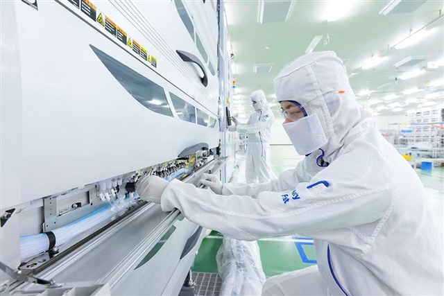
Tokyo Electron is a Japanese company that operates in the field of semiconductor equipment equipment. The company is an essential part of the global semiconductor supply chain, Without it, there would be no semiconductorsespecially advanced ones, because that is where they dominate the market.
Here on Getquin, a lot is written every day about the Dutch ASML $ASML (-2.1%) who have a monopoly in the field of EUV lithography. However, the EUV machine is unfortunately useless on its own, because each of ASML's highly complex EUV machines inevitably requires technology from Tokyo Electron. This concerns the coaters and developers.
With the coating an extremely thin layer of photoresist is applied to a wafer with nanometer precision, Only then are they usable for the EUV process. This is followed by developingin which specific exposed or unexposed areas on the wafer are removed in order to create a certain pattern. The whole process is incredibly complex and difficult to implement. The coater/developer and EUV machines form a kind of unit. Tokyo Electron has a market share of approx. 90% and even a monopoly in EUV lithography. monopoly. The barriers to entry are also considered to be very high. All in all, it can be said that there are no high-end chips without ASML's EUV lithography, but no EUV lithography without Tokyo Electron's coater/developer. Tokyo Electron benefits directly and inevitably from ASML's success.
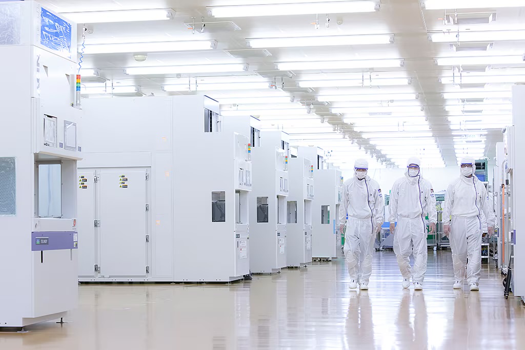
But that's not all, Tokyo Electron is much broader. They also hold market shares between 20-30% in dry etch, thin film deposition (CVD/ALD) and wafer cleaning (stable - rising everywhere). Competitors in this area are in particular Applied Materials $AMAT (-1.03%) and LAM Research $LRCX (+0.44%) .
Also becoming increasingly relevant is advanced packaging. Here, several chips are connected together, so to speak (e.g. CPUs, GPUs...). It therefore represents a key market for AI and other trends. Tokyo Electron currently holds market shares of around 10-15% (tendency strongly increasing). They are particularly strong in the essential wafer bondingi.e. the bonding of several finished wafers, where the market share is already at 32% (tendency rising sharply). They are also expanding into other areas.
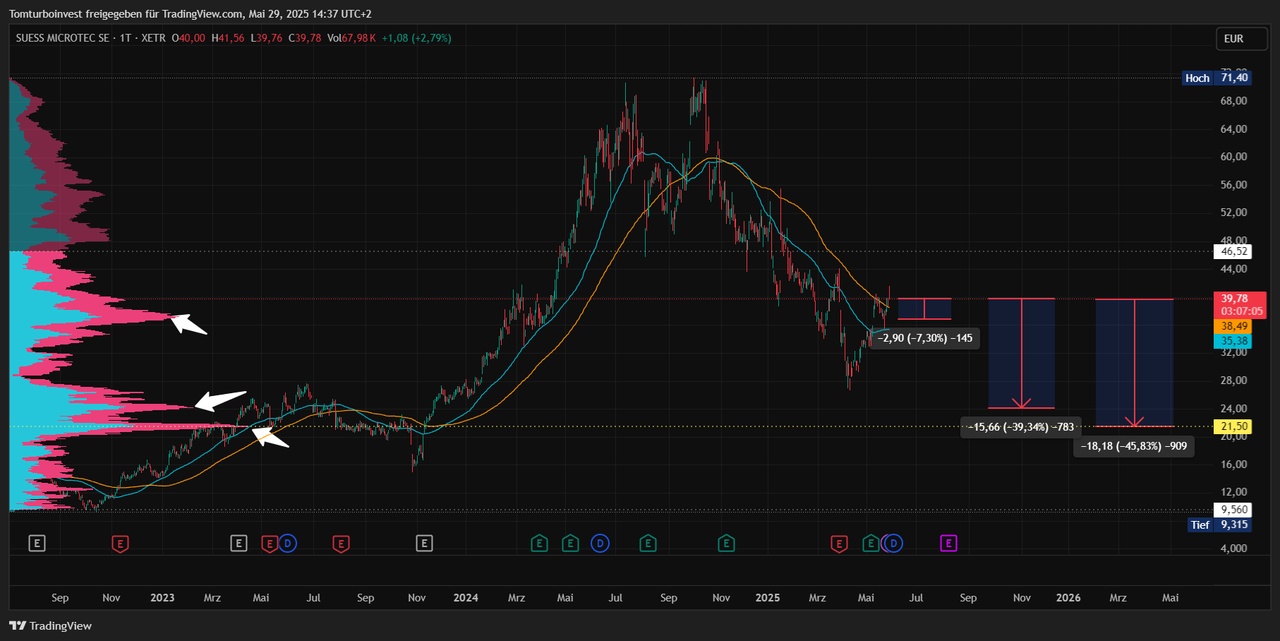
Overall, they benefit from their diversification and strong customer loyalty. They work very closely with foundry companies such as TSMC $2330 and Samsung $005930 whereby many processes are so closely coordinated that many innovations only emerge in production itself. Tokyo Electron also has an advantage over the competition, as their strong diversification (and market dominance in certain areas) means that they can offer complete solutions for their customers. In advanced packaging in particular, there are many smaller players that are only active in one niche (e.g. Süss MicroTec $SMHN (+0.71%) ), which makes them less competitive with Tokyo Electron.
It should now be roughly clear what kind of company Tokyo Electron is and why its products are so important. so important are so important. Now let's look at some numbers:
Turnover (2025): €14.9 billion (+32.83%)
Profit (2025): €3.3 billion (+49.50%)
Market capitalization: € 75.2 billion
P/E RATIO: 23.69
P/E ratio 2030e: 13.40
Debt: 0¥
Cash position: approx. € 3 billion
Over the next few years (up to 2030), Tokyo Electron is planning investments of 1.5 trillion ¥ (approx. €10 billion)especially in the area of Advanced Packaging. They are therefore investing heavily in their technological leadership and expanding into new growth markets. Their successful execution is reflected in the fact that they steadily becoming more profitable
and gaining market share all round. In the year 2027 they want a profit margin of 35% which would put the competition in the shade.
I also think it's important to emphasize that Tokyo Electron has been incredibly successful in talent acquisition acquisition. They are a very popular employer and last year alone they received 25,000 applications received from a total of around 17.000 employees worldwide. As part of their investment strategy, they plan to hire 2,000 new employees each year (10,000 in total) (this represents an increase of almost 60% growth). The employees who already work at Tokyo Electron are also very happy there. In Japan, only 1% of employees who start at Tokyo Electron leave the company at some point. Internationally it is also only 2-3%. This not only shows the quality of the employer, but also ensures that the know-how is retained within the company.
Conclusion: Tokyo Electron is a highly profitable, technological leader and innovative supplier whose products are irreplaceable, especially for the most advanced chip production. With a modern corporate culture and an aggressive growth strategy in an exponentially growing market environment the company offers an attractive investment opportunity with a robust moat and long-term high upside potential.
The savings plan is running :)
$STZ (-1.76%)
@Multibagger would that be something for you - a short long until $SMHN (+0.71%) shows clear tendencies? 😁
Edit: Weekly chart added @TradingMelone
$SMHN (+0.71%)
@Multibagger When I look at the charts according to my pattern, I am not surprised by the high short rate. For me, there is more downside than upside.
5-year view: Relevant volumes are all below the current price.
View since October - trend reversalThe price is currently running between VWAP and band 1 - for me no trend recognizable for a short-term trade, in any case wait until the price either approaches the VWAP or returns to band 2 (red line) at the bottom.
View since April - VWAP at last low: It looks similar, the price is hovering somewhere between Band1 and Band2 - currently no prominent entry point.
If I wanted to get in there, I would wait for a short-term trade until the price either runs back to the VWAP and this offers support in the short term, or wait for you as an old "short friend" until it runs back to the edge of Band2 (upper red line) and bounces off this resistance again.
But, this is just my interpretation according to my Setup🤷♂️
@Kundenservice Attaching pictures to comments would be a nice thing, I haven't followed the topic anymore, is something like that coming or is it planned?
What do you think of $SMHN (+0.71%) ?
@TomTurboInvest do you see potential there according to your approach? It is the most shorted share in the SDAX!
What do you think of $SMHN (+0.71%) ?
@TomTurboInvest do you see potential there according to your approach? It is the most shorted share in the SDAX!
Everyone has a problem child in their shopping cart, mine is $SMHN (+0.71%) .
What would you do with the security?
Thanks for your opinion !
Suss Microtec significantly exceeds its own 2024 targets + Trump and bitcoins + Today is a "small expiry day"
Suss Microtec $SMHN (+0.71%)Share gains significantly
Bitcoin $BTC (+1.45%)moves above $101,500 again
Friday: Stock market dates, economic data, quarterly figures
Small expiry day
08:00 UK: Retail Sales December FORECAST: 0.0% yoy/ n.a. previous: +0.2% yoy/+0.5% yoy
11:00 EU: Consumer prices December Eurozone PROGNOSE: +0.4% yoy/+2.4% yoy PREVIEW: +0.4% yoy/+2.4% yoy PREVIEW: -0.3% yoy/+2.2% yoy CORE RATE PROGNOSE: +0.5% yoy/+2.7% yoy PREVIEW: +0.5% yoy/+2.7% yoy PREVIEW: -0.6% yoy/+2.7% yoy
14:30 US: Housing starts/permits December housing starts FORECAST: +3.2% yoy previous: -1.8% yoy Building Permits FORECAST: -3.0% yoy previous: +6.1% yoy
15:15 US: Industrial production and capacity utilization December Industrial production PROGNOSE: +0.2% yoy previous: -0.1% yoy Capacity utilization PROGNOSE: 77.0% previous: 76.8%
From sand to chip: how is a modern semiconductor made?
Reading time: approx. 10min
1) INTRODUCTION
Since 2023 at the latest and the rapid rise of Nvidia $NVDA (-3.83%) semiconductors and "AI chips" in particular have been the talk of the town. Since then, investors have been chasing after almost every company that has something to do with the manufacture of chips, driving share prices to unimagined heights. However, hardly any investors really know how complex the value chain is within the production of modern chips.
In this article, I will give you an overview of the entire manufacturing process and the companies involved. Even if many of you have a vague idea that the production of modern chips is complex, you will certainly be surprised by how complex it really is in reality.
2) BASIC
The starting point for every chip are so-called wafers [1] - i.e. thin wafers, which usually consist of so-called high-purity monocrystalline silicon. In the field of power semiconductors, which primarily comprises chips for applications with higher currents and voltages, silicon carbide (SiC) or galium nitride (GaN) has recently also been used as the base material for the wafers.
In the so-called front end the actual core components of the chips - the so-called dies - are created and applied to the wafers. The dies are rectangular structures that contain the actual functionality of the later chip. The finished dies are then tested for their functionality and electrical properties. Each die that is found to be good is then integrated into the so-called backend where the individual dies are separated on the wafer. This is followed by the so-called packaging. The individual dies from the front end are then electrically contacted and integrated into a protective housing. In the end, this housing with the contacted die is what is usually called a chip chip.
Now that we have a rough overview of the overall process, let's take a closer look at the individual processes involved in producing the dies on the wafer. This is the area in which most highly complex machines are used and which is usually the most sensitive.
3) FROM SAND TO WAFER
Before wafers made of high-purity silicon can even be produced and the actual process for manufacturing dies can begin, the actual wafer must first be manufactured in almost perfect quality. To do this, quartz sand, which consists largely of silicon dioxide, is reduced with carbon at high temperatures. This produces so-called raw siliconwhich, with a purity of around 96%, is not yet anywhere near the quality required for the production of wafers.
In several chemical processes, which are carried out by Wacker Chemie
$WCH (-3.02%) or Siltronic
$WAF (-2.71%) are used to turn the "impure" silicon into so-called polycrystalline silicon with a purity of 99.9999999%. For every billion silicon atoms, there is then only one foreign atom in the silicon. However, this pure polycrystalline silicon is still not suitable for the production of wafers, as the crystal structure in the silicon is not uniform enough. In order to create the right crystal structure, the polycrystalline silicon is then melted again and a so-called ingotwhich is made from monocrystalline silicon is produced. A comparison between raw silicon and the ingot can be found in the following image [3]:
This ingot is then sawn into thin slices, which are then the final wafers for semiconductor production. The best-known wafer producers are Shin Etsu
$4063, (-1.08%)
Siltronic or GlobalWafers
$6488.
4) FROM THE WAFER TO THE DIE
The wafers described in the previous section can now be used to produce dies. The overall process for producing dies basically consists of applying a large number of layers using various chemical, mechanical and physical processes. The overall process (depending on the product) takes approx. 80 different layers on the wafer, requiring almost 1000 different process steps and 3 months
non-stop production are required [4].
A macroscopic analogy is useful here, which I have also taken from [4]. You can compare the overall process for producing dies with baking a large multi-layer cake. This cake has 80 layers and the recipe for baking consists of 1000 steps. It takes 3 months to make the cake and if even one layer of the cake deviates from the recipe by more than 1%, the whole cake collapses and has to be thrown away.
In the first process steps, the wafer is covered with billions tiny little transistors are created on the wafer, which are then all individually electrically contacted in the following steps. The final steps consist of electrically connecting the transistors to each other, resulting in a complete electrical circuit [4]:
Each individual layer of the approximately 80 layers in the die requires highly specialized processes, which can be roughly summarized as:
Apply masks
Ultimately, a mask can be thought of as an enlarged copy of the structure of a special layer in the die. These so-called photomasks are then scanned using so-called scanners or steppers "copied" in reduced size onto the wafer. The best-known manufacturer of such lithography systems is ASML
$ASML (-2.1%). It is currently the only producer of lithography systems that make it possible to produce structures smaller than 10 nanometers on the wafer. In today's powerful and modern chips, such as those found in smartphones, AI chips and processors, the smallest structures are around 3 nanometers in size. Other manufacturers of lithography systems for larger structures (10nm and larger) are Canon Electronics
$7739 or Nikon $7731 (-0.88%) .
The photomasks - i.e. the enlarged "copies" of the structures - are produced by companies such as Toppan $7911 (+0.85%) , Dai Nippon Printing
$7912 (-0.74%) or Hoya $7741 (-8.81%) manufactured. Systems for cleaning the photomasks or for applying the photoresist are produced, for example, by Suss Microtec
$SMHN (+0.71%) for example.
Apply/remove/modify/clean material
As can be seen in the overview above, there are a variety of methods and processes for modifying the material of a particular layer. As a result, there is a lot of different equipment that can handle a process very well with incredible specialization. The best-known and most successful equipment manufacturers include Applied Materials $AMAT (-1.03%), LAM Research
$LRCX (+0.44%), Tokyo Electron (TEL)
$8035, (-15.14%)
Suss Mictrotec, Entegris
$ENTG (-4.8%) and Axcelis $ACLS (-1%).
The material - for example, highly specialized chemicals - is of course also required for production. Companies such as Linde
$LIN (-1.71%), Air Liquide
$AI (-1.31%), Air Products
$APD (-2.97%) and Nippon Sanso
$4091 (-3.39%) are major manufacturers of process gases such as nitrogen, hydrogen and argon.
Inspect
As mentioned, every single layer in the manufacturing process of a die must be perfect in order to obtain a functional die at the end. Any small deviation or foreign particles can impair the functionality of the die. As the function of the die can only be checked precisely on the finished die, it is advantageous to inspect the individual layers for defects and deviations during production. Special machines are required for this, which must be able to do different things depending on the layer. Manufacturers of such machines include KLA
$KLAC (+0.01%) or Onto Innovation
$ONTO (-1.21%).
The following applies to almost all of the companies mentioned in this section: the companies are highly specialized and have quasi-monopolies on the machines for certain process steps. quasi-monopolies. Suitable equipment therefore usually costs several million dollars. In addition, some of the systems are so complex that they can only be serviced by the manufacturer's own service staff, which results in recurring service revenues for every machine sold. As a rule, each machine requires several highly specialized engineers to ensure long-term stable operation.
5) FROM THE DIE TO THE FINISHED CHIP
Once the wafer has been processed, the dies on the wafer are checked for functionality. There is highly specialized equipment for this, so-called probers. These probers test each individual chip several times, if necessary, to check the functionality implemented in the design. Manufacturers of such probers include Teradyne $TER (-4.99%), Keysight Technologies
$KEYS (-4.74%), Onto Innovation or Tokyo Electron. These probers have to control each individual die, some of which are only a few square millimetres in size, and contact the corresponding much smaller test structures with tiny needles. The testing process is sometimes outsourced to entire companies that offer die testing as a complete package. One example of such providers is Amkor Technology
$AMKR (-4.87%).
The processed and tested wafer is now sawn to obtain individual dies. The dies that are found to be good are then integrated into a protective housing in the backend. The dies that have not passed the functionality test are either sorted out or (depending on the error pattern) processed as a variant with reduced functionality similar to those with full functionality. After a final functional test in the package, the chip is ready for use.
6) FOUNDRIES, FABLESS & SOFTWARE
Now that we have an overview of the complex process of manufacturing a chip, let's zoom out a little further to understand which companies perform which tasks in the semiconductor industry.
It's funny that not once in the manufacturing process has the name Nvidia $NVDA (-3.83%) or Apple $AAPL (-5.14%) has been mentioned? Yet they have the most advanced chips, don't they?
The pure production of the chips is done by other companies - so-called foundries. Companies like Nvidia and even AMD $AMD (-3.71%) are in fact fablessThis means that they do not have their own production facilities but only supply the chip design and let the foundries manufacture the actual chip according to their design.
The design of a chip is like the blueprint for production - the foundries then take over the recipe creation and the actual production. There is special software for designing chips. Companies known for this software include Cadance Design
$CDNS (-3.72%) and Synopsys $SNPS (-3.85%). But also the industrial giant Siemens
$SIE (-4.7%) now also supplies software for designing integrated circuits. Synopsys also offers other software for data analysis within foundry production.
Speaking of foundries; the best known foundry is probably TSMC
$TSM, (-4.02%) which is the global market leader in foundries. TSMC designs itself no chips itself and specializes exclusively in the production of the most advanced generations of chips. Another major player that also masters the most advanced structure sizes is Samsung $005930. In contrast to TSMC manufactures Samsung also produces its own designs. Other large foundries are Global Foundries
$GFS, (-4.4%) which was originally a spin-off from AMD and the Taiwanese company United Micro Electronics
$UMC. (-1.67%)
The best-known fabless companies - i.e. companies without their own chip production - are Nvidia, Apple, AMD, ARM Holdings
$ARM, (-3.4%)
Broadcom $AVGO (-3.24%), MediaTek $2454 and Qualcomm $QCOM. (-0.57%) In the meantime Alphabet $GOOGL, (-2.86%)
Microsoft $MSFT, (-3.8%)
Amazon $AMZN (-7.55%) and Meta $META (-4.37%) have designed their own chips for certain functionalities and then have them manufactured in foundries.
In addition to foundries and fabless companies, there are of course also hybrid models, i.e. companies that take on both production and design. The best-known examples of this are, of course, companies such as Intel
$INTC (-3.75%) and Samsung. There is also a whole range of so-called Integrated Device Manufacturer (IDM)which for the most part only manufacture their own designed chips and do not accept customer orders for production. Well-known companies such as Texas Instruments
$TXN, (-1.51%)
SK Hynix
$000660,
STMicroelectronics
$STMPA, (-2.68%)
NXP Semiconductors
$NXPI, (-3.47%)
Infineon $IFX (-1.8%) and Renesas $6723 (-1.89%) are among the IDMs.
FINAL WORD
The aim of this article was to provide an overview of the complexity of the semiconductor industry. I do not, of course no claim to be complete, as there are of course many other companies that are part of this value chain. As Getquin thrives on active exchange, I'll give you some food for thought to discuss in the comments below the article:
In general, I can recommend the 20-minute YouTube video at [4] to any interested reader. It provides an excellent animated overview of the manufacturing process of modern chips.
Stay tuned,
Yours Nico Uhlig (aka RealMichaelScott)
SOURCES:
[1] Wikipedia: https://de.wikipedia.org/wiki/Wafer
[2] https://www.halbleiter.org/waferherstellung/einkristall/
[3] https://solarmuseum.org/wp-content/uploads/2019/05/solarmuseum_org-07917.jpg
[4] Branch Education on YouTube: "How are Microchips Made?" https://youtu.be/dX9CGRZwD-w?si=xeV0TYgJ2iwNOKyO
Good morning everyone,
Does anyone here happen to know why $SMHN (+0.71%) is currently being penalized?
Google didn't get me any further here.
Thank you very much!
Top creators this week