

$KDP (+6.77%)
$7751 (+0.6%)
$NXPI (+2.38%)
$WM (-3.53%)
$CDNS (-0.18%)
$BN (+0.46%)
$SOFI (+5.06%)
$UNH (+0.78%)
$AMT (-1.01%)
$UPS (+2.26%)
$BNP (+1.78%)
$NVS (-1.33%)
$DB1 (+0.13%)
$MSCI (+0.69%)
$ENPH (+1.15%)
$BKNG (+2.46%)
$LOGN (+1.87%)
$V (+0.35%)
$MDLZ (+1.11%)
$PYPL (+1.26%)
$000660
$MBG (+0.63%)
$BAS (-0.58%)
$UBSG (+1.33%)
$SAN (+1.91%)
$CVS (+0.85%)
$OTLY (+1.11%)
$GSK (+0.9%)
$ETSY (+2.31%)
$CAT (+0.5%)
$KHC (+1.01%)
$ADYEN (-0.93%)
$ADS (-0.12%)
$AIR (+0.57%)
$SBUX (+1.16%)
$CMG (-0.31%)
$META (+1.79%)
$KLAC (+3.21%)
$MELI (+5.8%)
$WOLF (+5.16%)
$GOOGL (+3.9%)
$EQIX (+0.47%)
$MSFT (+1.5%)
$CVNA (+0.85%)
$EBAY (+0.26%)
$005930
$6752 (-0.29%)
$KOG (-0.67%)
$VOW3 (+1.29%)
$GLE (-0.02%)
$LHA (-0.3%)
$STLAM (+0.33%)
$SPGI (+1.45%)
$MA (-0.06%)
$PUM (-0.8%)
$AIXA (+0.09%)
$FSLR (+2.13%)
$AAPL (+2.1%)
$REDDIT (+0.04%)
$AMZN (+1.47%)
$NET (+3.38%)
$MSTR (+1.56%)
$GDDY (+0%)
$TWLO (+1.43%)
$COIN (+1.29%)
$066570
$CL (-0.45%)
$ABBV (-0.41%)
$XOM (+0.15%)
- Markets
- Stocks
- KLA-Tencor Corp
- Forum Discussion
Discussion about KLAC
Posts
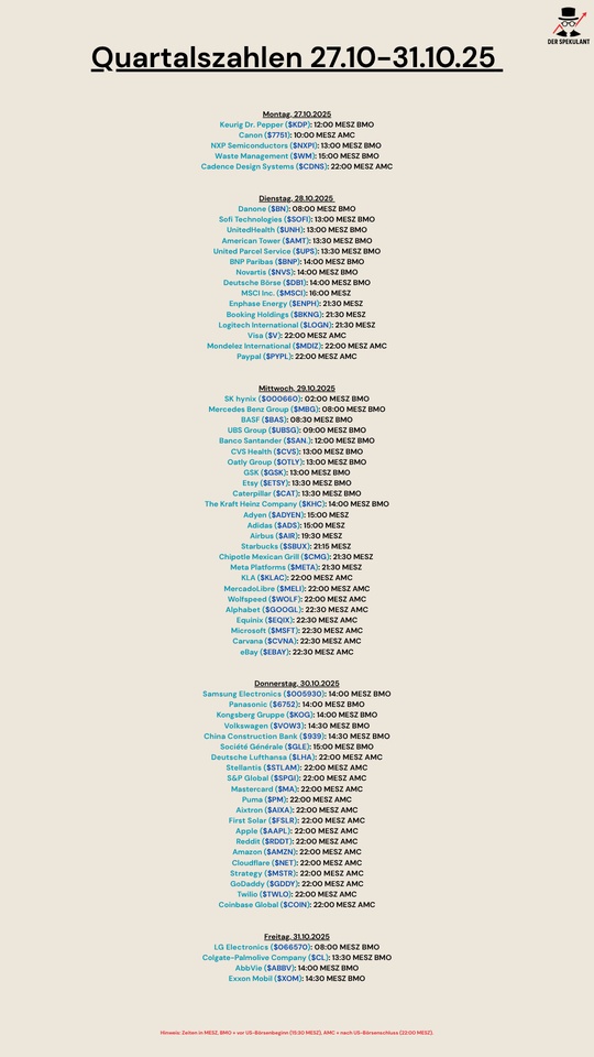
47Quarterly figures 27.10-31.10.25


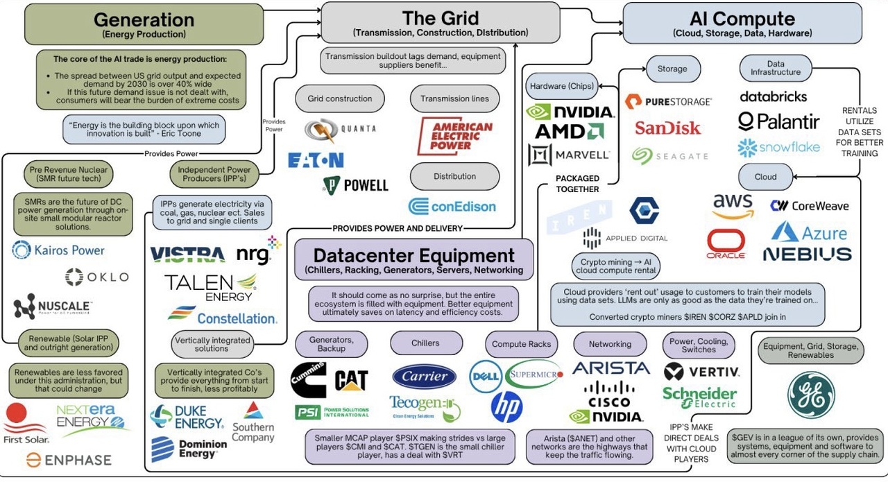
AI infrastructure continues to be one of the most exciting investment themes
$IREN (+2.38%)
$CIFR (-0.14%)
$BTC (-0.24%)
Maybe some exciting companies for you ✌️
I am currently only in $IREN (+2.38%) and $CIFR (-0.14%) which are the most promising for me in terms of the opportunity/return ratio. In the event of a further setback, I would $CIFR (-0.14%) probably add a little more and perhaps pick up one or two other companies.
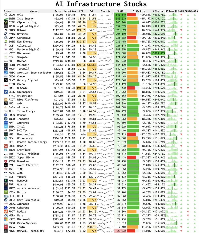
AI stocks, sorted by YTD performance:
Hyperscalers: $GOOGL (+3.9%)
$MSFT (+1.5%)
$AMZN (+1.47%)
$ORCL (-0.99%)
$BABA (+2.6%)
Neocloud: $NBIS (+7.43%)
$IREN (+2.38%)
$CRWV (+2.19%)
$APLD (+2.43%)
$GLXY (-7.87%)
$WYFI
Memory: $SNDK
$STX (-1.16%)
$MU (+0.51%)
$WDC (-1.94%)
$PSTG (+1.7%)
Semiconductor: $NVDA (+2.2%)
$AVGO (+2.23%)
$AMD (+2.11%)
$TSM (+1.08%)
$ASML (+1.87%)
$ARM (+4.7%)
$KLAC (+3.21%)
$INTC (+2.9%)
Networking: $CIEN (+2.12%)
$CLS (+10.78%)
$CRDO
$RMBS (-2.58%)
$ANET (+1.88%)
$APH (+1.19%)
$COHR (+5.62%)
Servers: $VRT (+3.58%)
$DELL (+2.29%)
$HPE (+2.97%)
Data: $INOD (+4.58%)
$PLTR (+2%)
$SNOW (+2.9%)
$DDOG (+1.03%)
$MDB (+1.81%)
Energy: $LEU (-4.89%)
$CEG
$OKLO
$TLNE
$GEV (-0.4%)
$NXT (+0%)
Batteries: $EOSE
$QS
$TSLA (+4.15%)
$MVST (-5.49%)
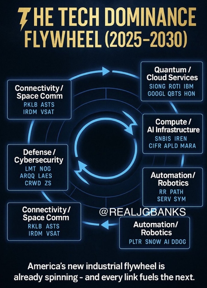
Every AI Value Chain explained:

In addition to $IREN and $CIFR also $GLXY, $INOD, $NVDA and $DDOG.
Plus $GOOGL, $AMZN and $BABA
So I'm pretty broadly positioned in this area when I look at it like this 😉😎
Others would say there is a cluster risk. However, the strategy of focusing on the highest possible returns means investing in the booming sectors, which at the moment are AI and commodities.

Time to take profits
After I recently sold my $AMZN (+1.47%) shares (which resulted in mostly negative feedback😉), my stop-limit order was also executed today at $KLAC (+3.21%) was executed today. You shouldn't get greedy and realize profits from time to time, especially if you are currently "over" invested in tech like me and we are constantly scratching the ATH.


Nova Ltd (ISIN IL0010845571): Analysis moat, margins and 10x potential
This report analyzes $NVMI, (+1.24%) an Israel-based provider of metrology and process control systems for the semiconductor industry. The company's current market capitalization is around USD 9.5 billion. To achieve a tenfold (10x) increase, Nova would have to grow to a valuation of USD 90 to 100 billion in the coming years.
I. First the summary
The path to 10x potential
Nova Ltd. is a critical technology enabler whose metrology solutions are imperative for the manufacture of advanced semiconductors (advanced nodes, 3D stacking). The central investment thesis for a tenfold increase is based on the exponential increase in metrology demand (dollar content per wafer) in advanced architectures such as High-Bandwidth Memory (HBM) and Gate-All-Around (GAA).
To reach the targeted market capitalization of USD 95 billion (maintaining the current high EV/Revenue multiple of 11.5x), Nova would need to achieve annual revenues of approximately USD 8.26 billion. This implies a compound annual growth rate (CAGR) of approximately 65% over five years (2025-2030), which is well above current consensus estimates (7.3% to 9.1%). The 10x potential is therefore theoretically feasible, but only through over-cyclical, structural growth in the HBM and ATM metrology niches.
The greatest risk is the high customer concentration and the inherent volatility of the semiconductor CapEx cycle.
II Business model and management
Nova Ltd (NVMI) develops and distributes metrology equipment for advanced process control in semiconductor manufacturing. Metrology is the essential quality control step that directly determines yield and profitability in miniaturization to 3nm or 2nm nodes.
The product portfolio includes metrology solutions for critical process steps such as lithography, etching, planarization (CMP), and advanced packaging. The most important areas are
Dimensional metrology: measurement of critical dimensions and alignment.
Film thickness and material metrology: Precise measurement of thin films.
Chemical metrology: Monitoring of chemical processes, critical for complex 3D architectures such as HBM.
Nova serves all major global manufacturing regions, including Israel, Taiwan, the United States, China and Korea.
The company was founded in 1993 by Giora Dishon (PhD in Materials Science) and Moshe Finarov (PhD in Semiconductor Physics), reflecting its technological depth. The current top management includes:
Gabriel Waisman President and CEO
Eitan Oppenhaim Executive Chairman of the Board
Dr. Shay Wolfling Chief Technology Officer (CTO)
The strategic leadership, supported by Dr. Wolfling, is driving the expansion of the Total Addressable Market (TAM) through targeted acquisitions, such as the acquisition of German ancosys GmbH in 2022, which strengthened the expertise in chemical metrology that is critical to HBM architectures. Remuneration (including restricted stock units) is geared towards the long-term commitment of management to the company's growth.
III The moat
Nova's moat is based on two main pillars: High switching costs and technological specialization.
Metrology systems are deeply integrated into the highly complex, automated production lines (Fabs). Replacing a qualified measurement tool is extremely costly, time consuming and jeopardizes critical yields in nanometer manufacturing. This deep integration creates high switching costs for customers and strengthens Nova's market position.
In the metrology market, which is dominated by market leader KLA Corporation (KLAC), Nova is positioning itself as a key challenger with an estimated 18 percent market share in the process control segment.
Nova's competitive advantage lies in its specialization in integrated metrology: measurements are taken directly during the process (real-time control).
Material metrology: expertise in dimensional and chemical monitoring.
The strength of this niche moat is reflected in its financial profitability:
Nova Ltd. $NVMI (+1.24%) / KLA Corporation $KLAC (+3.21%) / Lam Research $LRCX (+3.51%)
Market Share (Process Control) ~18% / ~55% / N/A
Operating Margin (TTM) 32.16% / 38.20% / 32.31%
Market capitalization (USD) $9.19B / $9.63B / $140.15B
The operating margin of 32.16% is on par with much larger industry players, demonstrating Nova's ability to command a price premium in its specialized niches.
IV. Margins and sales development
Nova's financial structure is characterized by high profitability and volatility inherent in the semiconductor cycle.
The company experienced strong sales growth during the post-pandemic chip boom (54.46% growth in 2021; 37.16% growth in 2022). The industry-wide CapEx decline led to a 9.25% drop in sales to USD 517.92 million in 2023.
However, the recovery is strong: last twelve months (LTM) revenue through Q2 2025 increased 43.69 percent to USD 807.09 million, demonstrating the critical nature of NVMI technology.
Profitability is stable and high, a strong indicator of the moat:
Gross Margin was exceptionally stable between 2017 and 2022, consistently above 54 percent, mostly above 55 percent.
The EBIT margin expanded significantly, from 16.18% (2019) to 27.01% (2021) and remained at 26.27% in 2022.
These high and rising margins demonstrate strong operating leverage. Any increase in sales in the next cycle (HBM/GAA) should lead to a disproportionately high increase in net profit.
V. Growth catalysts and investment conclusion
The 10x potential depends on the successful penetration of two structural technology trends: HBM revolution (high-bandwidth memory)
The AI boom is driving demand for HBM, whose market could grow to over USD 100 billion by 2030. HBM manufacturing requires extremely complex 3D stacking and advanced packaging. Nova reported record results in the HBM segment due to its leadership in chemical metrology. A leading memory manufacturer has also adopted the Nova Syntronics platform for key applications in HBM, as it offers unique solutions to problems such as wafer warpage in 3D structures.
The transition to the GAA architecture (from 2nm nodes) requires a multiplication of the metrology content per wafer, as the new transistor structures are much more complex. Nova expects the revenue acceleration from ATM starting in 2026, and the ability to deliver these new, precise measurements is the structural lever that expands Nova's TAM and accelerates growth beyond the pure CapEx cycle.
Nova Ltd. is structurally well positioned as a highly specialized niche player with high operating leverage and a technology-based moat to benefit from the increasing metrology demand in the semiconductor industry.
However, the share is already trading at a premium P/E of 43.81. The market is already pricing in strong growth. The tenfold potential (10x) is only achievable if Nova further expands its technological leadership in HBM and GAA and gains massive market share there, increasing sales growth forecasts from 9 percent to over 30-40 percent CAGR.
Successfully manages the risk of high customer concentration (over 10% sales from two main customers) and diversifies its customer base.
It is a high-risk bet on exponential technological growth, which requires continuous, flawless management execution to achieve the extremely high growth forecasts.
management to achieve the extremely high growth targets.
I will only buy here after a corresponding setback of at least 20%. What is your opinion?

New 52-week highs for these stocks
These shares reached a new 52-week high today:
Meta $META (+1.79%)
Broadcom $AVGO (+2.23%)
AMD $AMD (+2.11%)
Blackrock $BLK (-0.3%)
Astera Labs $ALAB (+1.4%)
Arista Networks $ANET (+1.88%)
Reddit $RDDT (-0.02%)
Lam Research $LRCX (+3.51%)
KLA Corp $KLAC (+3.21%)
S&P Global $SPGI (+1.45%)
Celsius $CELH
United Rentals $URI (-1.57%)
Do you hold one of the shares? If yes, congratulations!


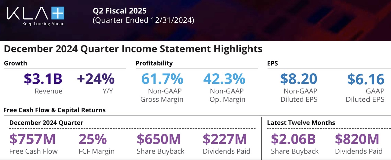


KLAC Q2'25 Earnings Highlights:
🔹 Revenue: $3.08B (Est. $2.94B) 🟢; UP +24% YoY
🔹 EPS: $8.20 (Est. $7.75) 🟢
Q3'25 Guidance:
🔹 Revenue: $2.85B-$3.15B (Est. $2.89B) 🟡
🔹 GAAP EPS: $7.45-$8.65 (Est. $7.50) 🟢
🔹 Non-GAAP EPS: $8.05 ± $0.60
Cash Flow & Shareholder Returns:
🔹 Gross Margin: 60.6% (Non-GAAP: 62.0%)
🔹 Net Income: $1.10B (Non-GAAP); $825M (GAAP)
🔹 Operating Cash Flow: $849.5M (Est. $906.26M) 🔴
🔹 Free Cash Flow: $757.2M (Est. $710.14M) 🟢
🔹 Capital Returns: $876.9M in Q2, $2.88B over last 12 months
Strategic & Business Highlights:
🔸 AI and high-performance computing demand driving semiconductor industry growth
🔸 Leading-edge investments gaining momentum, enabling growth for KLA
🔸 Strong cash generation & disciplined capital allocation continue to drive shareholder returns
CEO Rick Wallace's Commentary:
🔸 "Despite new U.S. government export controls, KLA delivered strong Q2 results, outperforming revenue expectations. AI and high-performance computing investments continue to expand, reinforcing our strategic positioning in an evolving semiconductor landscape."
Market Insights & Outlook:
🔸 Strong demand for semiconductor process control tools, aligning with next-gen chip manufacturing trends
🔸 Growth in AI and high-performance computing presents long-term opportunities for revenue expansion
🔸 Export restrictions remain a risk, but KLA continues to execute well within constraints

Diversification / sector breakdown
Hello everyone,
Yesterday showed me once again how important it is to invest across all sectors. Anyone who invests in individual stocks should "divide" their money into as many different sectors as possible.
Tech stocks did not do so well yesterday, in contrast to some classic blue chips such as $PEP (+0.32%) or $JNJ (-0.12%) . Even if these stocks are no longer a huge growth story, they give my portfolio stability in stormy times.
So I was still able to end the day on a positive note yesterday, even though I $AVGO (+2.23%) and $KLAC (+3.21%) etc. in my portfolio.
This was probably also due to the low weighting here and there, but I'm still happy about it and feel somehow confirmed that I'm on the right track with my "strategy".
These are my current thoughts on this....how did you see yesterday?
Greetings from DivGrowth1989 ;)

But in my opinion it's total nonsense. The two stocks have been going completely sideways for 3-4 years, while stocks like NVIDIA and Broadcom have risen massively. Sure, the keyword is AI hype, but I'd rather bet on something like that and take the risk of a -10% drop than a sideways movement for years and talk myself into the high dividend. I also have no idea that Jnj or Pepsi will outperform NVIDIA over the next few years.
But everyone as they feel comfortable👍

Semiconductor and power stocks fall today due to Deepseek panic
Semiconductor stocks and electricity shares are falling today because of the Deepseek panic. This panic is probably exaggerated. We'll talk about it in tonight's podcast. So be sure to subscribe to the podcast: https://open.spotify.com/show/3SHlvxmpYWkpiWnykajNPa
Semiconductors:
-12% Broadcom $AVGO (+2.23%)
-12% TSMC $2330
$TSM (+1.08%)
-11% Nvidia $NVDA (+2.2%)
-11% BE Semiconductor $SMH (+2.36%)
-11% ARM Holdings $ARM (+4.7%)
-11% ASML $ASML (+1.87%)
-9% Dell $DELL
$DELL (+2.29%)
-9% Micron $MU (+0.51%)
-6% AMD $AMD (+2.11%)
-5% KLA $KLAC (+3.21%)
Power stocks:
-20% Siemens Energy $ENR (+0.07%)
-15% Bloom Energy $BE (-1.06%)
-14% GE Vernova $GEV (-0.4%)
-13% Vistra $VST (-0.66%)
-11% Schneider Electric $SCHNEIDER
#deepseek
#openai
#ai
#ki
#china
#podcast
#spotify
$SPOT (+1.02%)
#semiconductor
#halbleiter


Trending Securities
Top creators this week