

Many shares are falling. This creates good entry opportunities again. Which shares do you have on your radar?
I am currently watching the following stocks:
Postes
49$SNPS (+2,1 %) Stocked up straight away, thanks Donald

Good morning dear Getquin community 👋
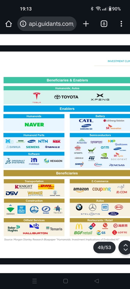
Today I would like to introduce you to The Humanoid 66 and what it's all about. The market for humanoid robotics is just taking off and is facing one of the biggest upheavals since the advent of the automobile. Morgan Stanley and Goldman Sachs expect the market to be worth between 38 billion and three trillion US dollars by 2035. By 2050, over 60 million humanoid robots could be in use in the USA alone.
With The Humanoid 66, Morgan Stanley has compiled a list of 66 companies that are likely to benefit directly or indirectly from this development. These include not only the manufacturers themselves, but also suppliers and technology groups that provide the necessary infrastructure, from semiconductor and battery producers to sensor technology and software through to platform operators for artificial intelligence.
The leading players include $TSLA (-3,07 %) Tesla with Optimus, Figure AI with Figure 02, Agility Robotics with Digit, Boston Dynamics with Atlas and Unitree with H1 and G1. Tesla is already planning to use more than a thousand Optimus robots in its own factories by 2024. The goal is clear: to make humanoid machines suitable for mass production at prices between 20,000 and 30,000 US dollars. Figure AI works closely with $MSFT (+0,63 %) Microsoft, OpenAI and $BMW (+0,67 %) BMW and was able to raise over 675 million US dollars in a financing round.
Technological progress is the key driver of this development. Multimodal generative AI enables humanoid robots to understand speech, communicate with humans and perform tasks autonomously. Advances in actuator technology, LiDAR systems, force sensors and battery technology are making the machines more efficient and more human-like. The energy density of modern lithium-ion cells is increasing by around 20 percent every two years, while the cost per kilowatt hour is expected to fall to 80 US dollars by 2030.
At the same time, wage costs for human labor are rising significantly. In the USA, they currently stand at just under 40 US dollars per hour, while in China they are around 6.50 US dollars and in India 4.45 US dollars. Studies show that automation can reduce labor costs in industrialized countries such as Germany, Japan and the USA by up to a third by 2025. Sectors such as agriculture, construction, care, logistics and manufacturing, where millions of jobs remain unfilled today, will be particularly affected.
The Humanoid 66 shows that this change goes far beyond individual companies. A new industrial ecosystem is emerging that links hardware, software, energy and data. Price reduction, scalability and integration into existing value chains will determine who will be among the winners.
Takeaway: Humanoid robotics is no longer a vision of the future, but the beginning of a structural reorganization of the global economy. Those who invest early in key areas such as AI chips, batteries, sensor technology and automation are positioning themselves in a sector that is likely to have a similarly profound impact as the invention of the car. The crucial question is just how far society is prepared to accept and integrate this new form of workforce.
For those who want to delve deeper: These are the companies featured in the Morgan Stanley report Humanoids @Tenbagger2024
@Multibagger
1. Tesla - USA - $TSLA (-3,07 %)
2. Toyota - Japan - $7203 (+0,82 %)
3. Xpeng - China - $XPEV (+0,81 %)
4. Naver - South Korea - (not listed)
5. CATL - China - $3750 (+2,68 %)
6. LG Energy Solution - South Korea - $373220 Subsidiary of LG
7. Samsung / Samsung SDI - South Korea - $SMSN (+0,52 %)
8. SK Innovation - South Korea - $096770
9. HD Hyundai Infracore / Doosan (component) - South Korea - $042670
10. Hengli Hydraulic - China - $601100
11. NTN - Japan - $6472 (+0,76 %)
12. NSK - Japan - $6471 (+1,35 %)
13. Sanhua - China - $002050
14. Siemens - Germany - $SIE (+1,06 %)
15. Top Group ("Topu") - China - $601689
16. Ambarella - USA - $AMBA (+2,55 %)
17. Synopsys - USA - $SNPS (+2,1 %)
18. NXP - Netherlands / USA - $NXPI (-0,53 %)
19. Qualcomm - USA - $QCOM (-0,49 %)
20. TSMC - Taiwan - $TSM (+1,4 %)
21. Wolfspeed - USA - $WOLF
22. ARM - UK - $ARM (+1,87 %)
23. onsemi - USA - $ON (-2,29 %)
24. cadence - USA - $CDNS (+2,6 %)
25. STMicroelectronics - Netherlands - $STM (-2,28 %)
26. NVIDIA - USA - $NVDA (+2,31 %)
27. SK hynix - South Korea - $HY9H (+8,78 %)
28. sociionext - Japan - $6526
29. SMIC - China - $0981
30. infineon - Germany - $IFX (-0,02 %)
31. Renesas - Japan - $6723 (-1,79 %)
32. Dassault Systèmes - France - $DSY (-3,76 %)
33. Mobileye - Israel / Intel ecosystem - $MBLY
34. Hexagon - Sweden - $HEXA B (+5,61 %)
35. Knight Transportation - USA - $KNX (+2,9 %)
36. DSV - Denmark - $DSV (-2,56 %)
37. Werner Enterprises - USA - $WERN (+0,85 %)
38. DHL Group - Germany / international - $DHL (-0,13 %)
39. Kuehne + Nagel - Switzerland - $KNIN (+0,46 %)
40. Obayashi - Japan - $1802 (+0,34 %)
41. China State Construction Engineering Corporation (CSCEC) - China - $601668
42. RBG (presumably an Asian construction company) - (not listed)
43. Shimizu - Japan - $1803 (+0,86 %)
44. Taisei - Japan - $1801 (-0,4 %)
45. Baker Hughes - USA - $BKR (-4,08 %)
46th SLB (Schlumberger) - USA - $SLB
47. Tenaris - Luxembourg / multinational - $TEN (-2,47 %)
48. Halliburton - USA - $HAL (-2,43 %)
49. amazon - USA - $AMZN (+1,56 %)
50th Coupang - South Korea $CPNG (+0,21 %)
51. JD.com - China - $JD (+0 %)
52. BMW - Germany - $BMW (+0,67 %)
53rd Mercedes-Benz - Germany - $MBG (+0,47 %)
54th General Motors - USA - $GM (+3,46 %)
55. BYD - China - $1211 (-0,58 %)
56. Stellantis - NL / multinational - $STLAM (+1,15 %)
57. Ford - USA - $F (+6,36 %)
58. McDonald's - USA - $MCD (-0,54 %)
59th Domino's - USA - $DPZ (-1,68 %)
60. BGF Retail - South Korea - $282330
61. GS Retail - South Korea - $007070
62nd Lotte - South Korea - $004990
63. Yum China - China - $YUMC (-1,8 %)
Source: Morgan Stanley Research Bluepaper Humanoids Investment Implications of Embodied AI and Stock3 drumbeat of Germany's humanoid robot manufacturers The Humanoid 66, 05.10.2025

What is your assessment and outlook for Synopsys $SNPS (+2,1 %) look like?
I bought it in the crash after the quarterly figures at a price of € 374
Thank you very much for your assessment and have a nice holiday
LG

A lot has happened in my portfolio again in recent weeks. In addition to a few sales (including $GOOGL (+1,8 %) and $NVDA (+2,31 %)) from hot sectors, I have built up cash and diversified further ($CMG (-1,83 %)
$SNPS, (+2,1 %)
$BRO (-0,27 %)
$AMGN (-0,04 %)
$LSEG (+4,15 %)). Further acquisitions and new entries (e.g. $INTU (+1,64 %)
$ADP (-0,26 %)
$WM (-0,38 %)
$CTAS (+0,02 %)
$RMS (-1 %)) are planned. As short- to medium-term trades, I have invested in $Adobe (-0,07 %) and $TTD (-3,92 %) as short to medium-term trades. I mainly invest for the long term, but a correction (technology, cloud) including sector rotation (consumer, pharma, software) seems inevitable to me. I am therefore taking a wait-and-see approach and, if necessary, I will reenter $GOOGL (+1,8 %) and $NVDA (+2,31 %) again at the appropriate time.
Please let me know what you think.
I will probably share future updates with you every two months at the beginning of the month (November, January,...).
I wish you all a successful time.

Unfortunately in completely brainless denominations, because my adorable girlfriend kept chatting to me while I was buying it and I mistyped it :D
To be honest, I don't know why people keep saying "the market has run hot" when actually every few days some new stock is completely slaughtered.
I didn't catch a low, the countermovement is underway. In any case, this will not be the last time I buy. The savings plan is also still running.

$SNPS (+2,1 %) Position doubled 😁 Patience has never been my Stärke🤷🏼♂️
if it should fall further I will continue to buy ✌️

$SNPS (+2,1 %) with massive dip, now at a price level not see since april 2023. Could be a good point of entry.... opinions? targets missed but for long-term investment it seems promising with chips and robotics
Meilleurs créateurs cette semaine


