
Reading time: approx. 10min
1) INTRODUCTION
Since 2023 at the latest and the rapid rise of Nvidia $NVDA (-0,93 %) semiconductors and "AI chips" in particular have been the talk of the town. Since then, investors have been chasing after almost every company that has something to do with the production of chips, driving share prices to unimagined heights. However, hardly any investors really know how complex the value chain is within the production of modern chips.
In this article, I will give you an overview of the entire production process and the companies involved. Even if many of you have a vague idea that the production of modern chips is complex, you will certainly be surprised by how complex it really is in reality.
2) BASIC
The starting point for every chip are so-called wafers [1] - i.e. thin wafers, which usually consist of so-called high-purity monocrystalline silicon. In the field of power semiconductors, which primarily comprises chips for applications with higher currents and voltages, silicon carbide (SiC) or galium nitride (GaN) has recently also been used as the base material for the wafers.
In the so-called front end the actual core components of the chips - the so-called dies - are created and applied to the wafers. The dies are rectangular structures that contain the actual functionality of the later chip. The finished dies are then tested for their functionality and electrical properties. Each die that is found to be good is then integrated into the so-called backend where the individual dies are separated on the wafer. This is followed by the so-called packaging. The individual dies from the front end are then electrically contacted and integrated into a protective housing. In the end, this housing with the contacted die is what is usually called the chip chip.
Now that we have a rough overview of the overall process, let's take a closer look at the individual processes involved in producing the dies on the wafer. This is the area in which most highly complex machines are used and which is usually the most sensitive.
3) FROM SAND TO WAFER
Before wafers made of high-purity silicon can even be produced and the actual process for manufacturing dies can begin, the actual wafer must first be manufactured in almost perfect quality. To do this, quartz sand, which consists largely of silicon dioxide, is reduced with carbon at high temperatures. This produces so-called raw siliconwhich, with a purity of around 96%, is not yet anywhere near the quality required for the production of wafers.
In several chemical processes, which are carried out by Wacker Chemie
$WCH (-1,14 %) or Siltronic
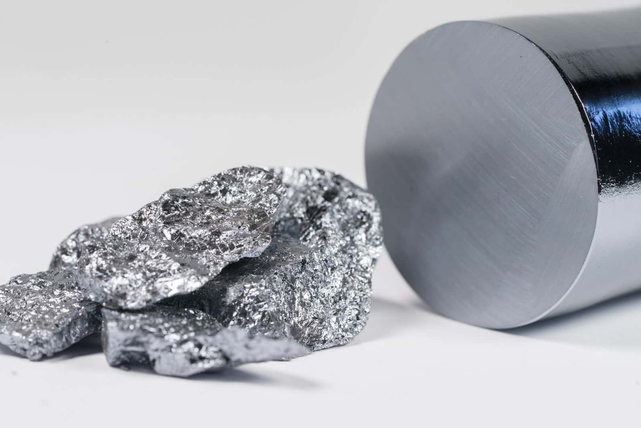
$WAF (-1,05 %) are used to turn the "impure" silicon into so-called polycrystalline silicon with a purity of 99.9999999%. For every billion silicon atoms, there is then only one foreign atom in the silicon. However, this pure polycrystalline silicon is still not suitable for the production of wafers, as the crystal structure in the silicon is not uniform enough. In order to create the right crystal structure, the polycrystalline silicon is then melted again and a so-called ingotwhich is made from monocrystalline silicon is produced. A comparison between raw silicon and the ingot can be found in the following image [3]:
This ingot is then sawn into thin slices, which are then the final wafers for semiconductor production. The best-known wafer producers are Shin Etsu
$4063, (-9,66 %)
Siltronic or GlobalWafers
$6488.
4) FROM THE WAFER TO THE DIE
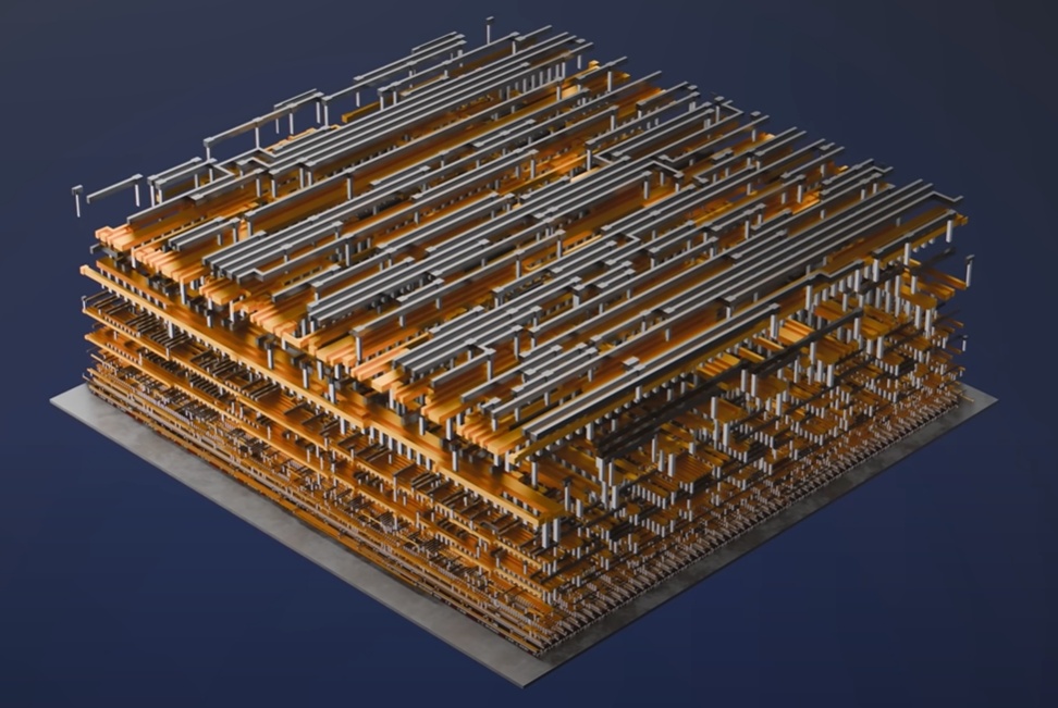
The wafers described in the previous section can now be used to produce dies. The overall process for producing dies basically consists of applying a large number of layers using various chemical, mechanical and physical processes. The overall process (depending on the product) takes approx. 80 different layers on the wafer, requiring almost 1000 different process steps and 3 months
non-stop production are required [4].
A macroscopic analogy is useful here, which I have also taken from [4]. You can compare the overall process for producing dies with baking a large multi-layer cake. This cake has 80 layers and the recipe for baking it consists of 1000 steps. It takes 3 months to make the cake and if even one layer of the cake deviates from the recipe by more than 1%, the whole cake collapses and has to be thrown away.
In the first process steps, the wafer is covered with billions tiny little transistors are created on the wafer, which are then all individually electrically contacted in the following steps. The final steps consist of electrically connecting the transistors to each other, resulting in a complete electrical circuit [4]:
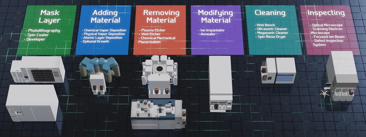
Each individual layer of the approximately 80 layers in the die requires highly specialized processes, which can be roughly summarized as:
- Applying masks: Photolithography, photoresist coating (applying photoresist)
- Apply material: Chemical Vapor Deposition (CVD), Physical Vapor Deposition (PVD), Atomic Layer Deposition
- Remove material: Plasma annealing, Wet annealing, Chemical Mechanical Planarization (CMP)
- Modify material: Ion Implanting, Annealing
- Material cleaning
- Inspecting the layers: Optical, Microscopical, Focused Ion Beam, Defect Inspection
Apply masks
Ultimately, a mask can be thought of as an enlarged copy of the structure of a special layer in the die. These so-called photomasks are then scanned using so-called scanners or steppers "copied" in reduced size onto the wafer. The best-known manufacturer of such lithography systems is ASML
$ASML (-3,54 %). It is currently the only producer of lithography systems that make it possible to produce structures smaller than 10 nanometers on the wafer. In today's powerful and modern chips, such as those found in smartphones, AI chips and processors, the smallest structures are around 3 nanometers in size. Other manufacturers of lithography systems for larger structures (10nm and larger) are Canon Electronics
$7739 or Nikon $7731 (+1,95 %) .
The photomasks - i.e. the enlarged "copies" of the structures - are produced by companies such as Toppan $7911 (-1,15 %) , Dai Nippon Printing
$7912 (-0,3 %) or Hoya $7741 (-1,05 %) manufactured. Systems for cleaning the photomasks or for applying the photoresist are produced, for example, by Suss Microtec
$SMHN (-2,8 %) for example.
Apply/remove/modify/clean material
As can be seen in the overview above, there are a variety of methods and processes for modifying the material of a particular layer. As a result, there is a lot of different equipment that can handle a process very well with incredible specialization. The best-known and most successful equipment manufacturers include Applied Materials $AMAT (-6,4 %), LAM Research
$LRCX (-6,1 %), Tokyo Electron (TEL)
$8035, (-5,28 %)
Suss Mictrotec, Entegris
$ENTG (-4,22 %) and Axcelis $ACLS (-5,19 %).
The material - for example, highly specialized chemicals - is of course also required for production. Companies such as Linde
$LIN (+0,99 %), Air Liquide
$AI (+0,13 %), Air Products
$APD (+2,05 %) and Nippon Sanso
$4091 (-0,06 %) are major manufacturers of process gases such as nitrogen, hydrogen and argon.
Inspect
As mentioned, every single layer in the manufacturing process of a die must be perfect in order to obtain a functional die at the end. Any small deviation or foreign particles can impair the functionality of the die. As the function of the die can only be checked precisely on the finished die, it is advantageous to inspect the individual layers for defects and deviations during production. Special machines are required for this, which must be able to do different things depending on the layer. Manufacturers of such machines include KLA
$KLAC (-5,5 %) or Onto Innovation
$ONTO (-6,73 %).
The following applies to almost all of the companies mentioned in this section: the companies are highly specialized and have quasi-monopolies on the machines for certain process steps. quasi-monopolies. Suitable equipment therefore usually costs several million dollars. In addition, some of the systems are so complex that they can only be maintained by the manufacturer's own service staff, which ensures recurring service revenue for every machine sold. As a rule, each machine requires several highly specialized engineers to ensure long-term stable operation.
5) FROM THE DIE TO THE FINISHED CHIP
Once the wafer has been processed, the dies on the wafer are checked for functionality. There is highly specialized equipment for this, so-called probers. These probers test each individual chip several times, if necessary, to check the functionality implemented in the design. Manufacturers of such probers include Teradyne $TER (-6,82 %), Keysight Technologies
$KEYS (-2,45 %), Onto Innovation or Tokyo Electron. These probers have to control each individual die, some of which are only a few square millimetres in size, and contact the corresponding much smaller test structures with tiny needles. The testing process is sometimes outsourced to entire companies that offer die testing as a complete package. One example of such providers is Amkor Technology
$AMKR (-1,83 %).
The processed and tested wafer is now sawn to obtain individual dies. The dies that are found to be good are then integrated into a protective housing in the backend. The dies that have not passed the functionality test are either sorted out or (depending on the error pattern) processed as a variant with reduced functionality similar to those with full functionality. After a final functional test in the package, the chip is ready for use.
6) FOUNDRIES, FABLESS & SOFTWARE
Now that we have an overview of the complex process of manufacturing a chip, let's zoom out a little further to understand which companies perform which tasks in the semiconductor industry.
It's funny that not once in the manufacturing process has the name Nvidia $NVDA (-0,93 %) or Apple $AAPL (+4,07 %) has been mentioned? Yet they have the most advanced chips, don't they?
The pure production of the chips is done by other companies - so-called foundries. Companies like Nvidia and even AMD $AMD (-5,76 %) are in fact fablessThis means that they do not have their own production facilities but only supply the chip design and let the foundries manufacture the actual chip according to their design.
The design of a chip is like the blueprint for production - the foundries then take over the recipe creation and the actual production. There is special software for designing chips. Companies known for this software include Cadance Design
$CDNS (-1,22 %) and Synopsys $SNPS (+0 %). But also the industrial giant Siemens
$SIE (+1,02 %) now also supplies software for designing integrated circuits. Synopsys also offers other software for data analysis within foundry production.
Speaking of foundries; the best known foundry is probably TSMC
$TSM, (-3,01 %) which is the global market leader in foundries. TSMC designs itself no chips itself and specializes exclusively in the production of the most advanced generations of chips. Another major player that also masters the most advanced structure sizes is Samsung $005930. In contrast to TSMC manufactures Samsung also produces its own designs. Other large foundries are Global Foundries
$GFS, (-7,08 %) which was originally a spin-off from AMD and the Taiwanese company United Micro Electronics
$UMC. (-7,08 %)
The best-known fabless companies - i.e. companies without their own chip production - are Nvidia, Apple, AMD, ARM Holdings
$ARM, (-11,76 %)
Broadcom $AVGO (-2,79 %), MediaTek $2454 and Qualcomm $QCOM. (-2,91 %) In the meantime Alphabet $GOOGL, (+0,35 %)
Microsoft $MSFT, (-0,01 %)
Amazon $AMZN (-1,07 %) and Meta $META (-1,77 %) have designed their own chips for certain functionalities and then have them manufactured in foundries.
In addition to foundries and fabless companies, there are of course also hybrid models, i.e. companies that take on both production and design. The best-known examples of this are, of course, companies such as Intel
$INTC (-15,74 %) and Samsung. There is also a whole range of so-called Integrated Device Manufacturer (IDM)which for the most part only manufacture their own designed chips and do not accept customer orders for production. Well-known companies such as Texas Instruments
$TXN, (-1,73 %)
SK Hynix
$000660,
STMicroelectronics
$STMPA, (-3,38 %)
NXP Semiconductors
$NXPI, (-1,97 %)
Infineon $IFX (-3,16 %) and Renesas $6723 (-3,68 %) are among the IDMs.
FINAL WORD
The aim of this article was to provide an overview of the complexity of the semiconductor industry. I do not, of course no claim to be complete, as there are of course many other companies that are part of this value chain. As Getquin thrives on active exchange, I'll give you some food for thought to discuss in the comments below the article:
- feel free to link any other companies in the comments if you think I've forgotten any relevant ones
- what was the most surprising new information for you from the article?
- which companies from the article have you never heard of?
- before reading the article, did you know approximately how a modern chip is produced and what steps are necessary for this?
In general, I can recommend the 20-minute YouTube video at [4] to any interested reader. It provides an excellent animated overview of the manufacturing process of modern chips.
Stay tuned,
Yours RealMichaelScott
SOURCES:
[1] Wikipedia: https://de.wikipedia.org/wiki/Wafer
[2] https://www.halbleiter.org/waferherstellung/einkristall/
[3] https://solarmuseum.org/wp-content/uploads/2019/05/solarmuseum_org-07917.jpg
[4] Branch Education on YouTube: "How are Microchips Made?" https://youtu.be/dX9CGRZwD-w?si=xeV0TYgJ2iwNOKyO